


Introduction
The demand to connect several devices to the wireless network at once has arisen as a result of the recent advancements in mobile devices and communications technology [Reference Andrews, Buzzi, Choi, Hanly, Lozano, Soong and Zhang1]. In order to achieve this requirement, the Federal Communications Commission (FCC) has currently chosen the frequency range of 25–70 GHz for the upcoming generations of mobile communication, which is called fifth-generation (5G) communication technology [Reference Sheet2, Reference Pi and Khan3]. 5G technology offers faster data speeds, greater dependability, low-power connectivity for millions of devices, and support for cutting-edge innovations like driverless cars, smart cities, and virtual reality [Reference Thompson, Ge, Wu, Irmer, Jiang, Fettweis and Alamouti4]. In addition, the 5G communication devices are compact, and they require small antennas for better performance. A planar configuration can achieve compactness, but it suffers from low gain and radiation efficiency. One of the techniques to achieve high gain is to use frequency-selective and metasurface reflectors behind the radiation element. Many researchers have designed different frequency-selective surfaces (FSSs) and metasurface-based antennas for high-gain 5G communication devices. Some of the previously published metasurface-based antenna designs are discussed in the next few paragraphs.
In [Reference Hussain, Jeong, Abbas, Kim and Kim5], the authors designed a multilayer, low-profile, circularly polarized (CP) wideband patch antenna for 5G communication systems. The presented antenna design consists of a slot-loaded modified rectangular patch element, an array of metasurfaces, and a ground plane. The patch element was sandwiched between the ground plane and the metasurface. It was observed that the proposed antenna offered an impedance bandwidth of 34.7% from 24 to 34.1 GHz with a maximum gain of 11 dBi. In [Reference Tariq, Naqvi, Hussain and Amin6], a metasurface was employed to enhance the isolation between the multiple-input multiple-output (MIMO) antennas as well as to achieve high gain. It was noted that the incorporation of a metasurface layer above the MIMO antenna enhanced the gain up to 10.27 dBi. The same kind of MIMO configuration was presented in [Reference Sehrai, Asif, Shah, Khan, Ullah, Ibrar, Jan, Alibakhshikenari, Falcone and Limiti7], in which the authors achieved a gain of 10.44 dBi. In [Reference Ferreira-Gomes, Oliveira and Mejía-Salazar8], a chiral metasurface integrated broadband CP patch antenna was designed for millimeter-wave (mmWave) applications. The presented results demonstrated that the antenna had an impedance bandwidth of 22.6% (25.3–31.6 GHz) and a peak gain of 8 dBi. In [Reference Kumar, Ghosh and Saha9], a patch antenna design was presented for high-gain 28 GHz applications. To enhance the gain of the patch antenna,  $15 \times 15$ element array of multilayer metasurface was utilized. From the presented configuration, the authors achieved a gain of about 16.7 dBi in the band of interest.
In [Reference Althuwayb10], a slotted bowtie antenna was designed using metamaterial and substrate-integrated waveguide (SIW) technology. To realize compactness, the metamaterial and SIW were implemented by using trapezoidal slots on the top surface of the antenna and metallic via holes through the substrate layer. For improved performance, an artificial magnetic conductor (AMC) was used. The results showed that the antenna offers a gain and radiation efficiency of 5.5 dBi and 66.5%, respectively. In [Reference Abdelaziem, Ibrahim and Abdalla11], near-zero index metasurface structure was designed for the gain enhancement of patch antenna. A  $2\times 2$ array of a designed metasurface was placed above the patch antenna and realized a peak gain of 13.3 dBi at 26 GHz. In [Reference Yi, Mu, Han and Li12], a broadband aperture-coupled slotted-mushroom metasurface antenna was designed for 28 GHz applications. For suppressed backward radiation, a printed ridge gap waveguide (PRGW) technology with a perfect magnetic conductor (PMC) shielding was used underneath the microstrip feeding line, which improved the front-to-back ratio by 16 dB and enhanced the gain up to 19.2 dBi. In [Reference Gorai, Deb, Panda and Ghatak13], a cavity-backed tri-band SIW-based slot antenna design for mmWave applications was presented. By etching a modified spiral slot resonator from the radiating element, a tri-band response was achieved. The performance of the proposed antenna was further enhanced by placing an array of metasurfaces above the antenna. The presented antenna exhibited maximum radiation efficiencies of 88.37%, 88.63%, and 89.85% in the operating bands, while the peak gains were noted to be 7, 8.5, and 14.5 dBi, respectively.
Although the above-reported antenna designs offered good performance in terms of gain, the multilayer configuration may restrict their use in compact communication devices. Furthermore, most of the antennas, whether designed for a single frequency band or multiple frequencies, have not reported or designed a wideband metasurface-based antenna for mmWave applications. In this paper, an effort has been made to design a compact, wideband, high-gain, and directional planar antenna for mmWave applications. For reduced antenna dimensions, the meandering radiating element is designed on a loss-low dielectric substrate. The partial ground plane with parasitic elements (placed on the backside of the substrate) is used to achieve a wide impedance bandwidth ranging from 23 to 38.8 GHz. One of the major objectives of the design is to get high gain and directional radiation characteristics, which are achieved by incorporating a wideband metasurface behind the designed planar antenna. The integration of the metasurface led to an average gain of 6.99 dBi and directional radiation performance in the operating bandwidth. The complete antenna design procedure and its results are presented in the upcoming sections.
Metasurface-based planar antenna
Before explaining the design of the proposed metasurface-based antenna, the design of the radiating element and metasurface are discussed in detail in the below-mentioned sections.
Meandered planar antenna
The design of the proposed wideband planar antenna is illustrated in Fig. 1, while the design parameters used to build the antenna are listed in Table 1. The antenna is designed on a low-loss and flexible Rogers RT/Duroid 5880 substrate. The thickness of the substrate for the antenna design is chosen to be 0.254 mm. One can note from the design shown in Fig. 1(a) that the proposed antenna is composed of a meander-shaped patch radiator fed using a 50 Ω microstrip feeding line. The length of the one meandering section is equal to one guided wavelength at 26 GHz. The back side of the antenna comprises a partial ground plane (see Fig. 1b), which is utilized to achieve wide impedance bandwidth. It is also observed from Fig. 1(b) that  $3\times 3$ array of parasitic elements is placed right behind the radiating element, whose main purpose is to provide better impedance matching in the operating bandwidth.

Figure 1. Design of the proposed planar wideband antenna: (a) front side and (b) back side.
Table 1. Design parameters used for the construction of a planar wideband antenna (all dimensions in mm)

The effect of parasitic elements on the antenna performance is shown in Fig. 2, where the reflection coefficient (S 11) response of the proposed antenna is plotted. One can note that without parasitic elements, the antenna offers an impedance bandwidth of 15.02 GHz in the frequency range of 23.72–38.74 GHz, as shown in Fig. 2. On the other hand, the use of parasitic elements increased the upper frequency limit of the antenna by 1.12 GHz (see Fig. 2) and also increased the lower frequency limit by 580 MHz, as shown in Fig. 2. This increase in the frequency limit tends to achieve an impedance bandwidth of 16.72 GHz.

Figure 2. S 11 of the proposed planar wideband antenna without and with parasitic elements.
The effect of different parasitic element configurations on the planar antenna S 11 and realized gain is shown in Fig. 3. For  $3 \times 3$ and
  $4\times 3$ parasitic arrays, the antenna offers better impedance matching compared to
  $3\times 5$ and
  $4\times 5$ arrays, as shown in Fig. 3(a). In the case of
  $4 \times 3$ array, a shift in frequency is observed. On the other hand, different arrays have a minor effect on the gain of the antenna (see Fig. 3b).

Figure 3. (a) S 11 and (b) realized gain of the planar wideband antenna for different parasitic element configurations.
The simulated antenna efficiency and realized gain are shown in Fig. 4. As shown in Fig. 4(a), the radiation efficiency of the proposed antenna is >95% for the operating frequency range, while the total efficiency fluctuates in the range of 78–97%. On the other hand, the gain of the antenna varies in the range of 4-6.93 dBi in the entire operating range (see Fig. 4b).

Figure 4. (a) Radiation efficiency, total efficiency, and (b) realized gain of the proposed planar wideband antenna.
Figure 5 depicts the radiation characteristics of the proposed antenna for both the yz- and xz-planes at various frequencies. The results show that the proposed planar antenna has a typical monopole-like radiation pattern for the yz-plane. In the case of 24 GHz, the yz-plane main beam is aimed at 210∘, indicating that the antenna is radiating backward. The xz-plane pattern, on the other hand, is noted to be quasi-omnidirectional for frequencies up to 32 GHz, as shown in Fig. 5(a–c). This pattern becomes bi-directional at higher frequencies (see Fig. 5d). This change in the radiation pattern may be associated with the coupling effect of parasitic elements.

Figure 5. Far-field radiation characteristics of the proposed planar wideband antenna at (a) 24 GHz (b) 28 GHz (c) 32 GHz, and (d) 36 GHz.
To improve the radiation characteristics of the proposed antenna, a metasurface reflector is designed, whose details are provided in the following subsection.
Metasurface design
Figure 6 shows the front view of the proposed metasurface reflector. It is designed on a low-loss Rogers RT/Duroid 5880 dielectric substrate having a thickness of 1.57 mm. One can observe from the figure that a square split ring resonator (SRR) along with a circular SRR are used to design the metasurface, while the backside consists of a full ground plane. The other design parameters are as follows:  $W_M = 4$,
  $L_{p1} = 3.5$,
  $R_{\rm in} = 0.55$,
  $d_1 = 0.6$,
  $d_2 = 0.2$,
  $g_1 = 0.8$, and
  $g_2 = 0.4$ (all dimensions in millimeter).

Figure 6. Proposed metasurface design.
In a SRR, the applied electric field is parallel to the no-split-bearing side and generates electric current on the same side only. On the contrary, when the electric field is applied along a split bearing side, it causes an electric current in the same side as well as the perpendicular (no split) side. Using this technique, two gaps are introduced in the adjacent sides of the square SRR, one for each linearly polarized impinging field. The inner circular SRR is used to generate plasmon resonances at higher frequencies, thereby achieving a wider bandwidth.
The metasurface is simulated in CST Microwave Studio by using periodic boundary conditions. Electric and magnetic fields are used in the x and yaxes, respectively, while floquet port is used in the +z axis. The simulated S-parameters of the proposed metasurface are depicted in Fig. 7. It can be observed that the metasurface is operating well from 11 to 35 GHz, according to the −3 dB bandwidth criteria, which covers the operating band of interest.

Figure 7. S-parameters of the proposed metasurface.
Planar antenna integrated with metasurface
After designing the metasurface, the proposed antenna design presented in the subsection “Meandered Planar Antenna” is integrated to achieve high gain and directional radiation characteristics. The configuration of the proposed metasurface integrated planar antenna is shown in Fig. 8. When the antenna is located at a specific distance over the metasurface reflector, the metasurface reflects the backward radiation of the antenna to the opposite side. Therefore, two wave components will be added in the same phase, which gives constructive interference and ultimately improves radiation performance. Let us consider that ϕ t and ϕ r are the phases of the transmitted and reflected waves, and the complete propagation trip between metasurface reflector is denoted by ϕ s. Mathematically, these phases can be related as
 \begin{equation}
\phi_{\rm t} = \phi_{\rm r} + \phi_{\rm s}
\end{equation}
\begin{equation}
\phi_{\rm t} = \phi_{\rm r} + \phi_{\rm s}
\end{equation}and
 \begin{equation}
\phi_{\rm s} = 4\pi f \times \frac{t}{c},
\end{equation}
\begin{equation}
\phi_{\rm s} = 4\pi f \times \frac{t}{c},
\end{equation}where c is the speed of light, t is the gap between antenna and metasurface, and ϕ t should be 0 or the integral of 2π [Reference Das and Mandal14].

Figure 8. Configuration of the metasurface integrated planar antenna.
In the proposed design, the metasurface is placed beneath the designed antenna so that it makes the back radiation of the antenna in phase and then enhances the gain. In this scenario, an important factor is the distance between the antenna and the metasurface reflector, which ensures the constructive interference of directly radiated and reflected waves. To estimate the spacing between both of them, the following equation can be used [Reference Yuan, Xi and Zhao15]:
 \begin{equation}
\phi_{\rm Metasurface} -2\beta t = 2n\pi,
\end{equation}
\begin{equation}
\phi_{\rm Metasurface} -2\beta t = 2n\pi,
\end{equation}where π represents the reflected wave phase from the metasurface layer and β is the free-space propagation constant, which is equal to  $2\pi/\lambda_0$, where λ 0 is the free-space wavelength at 28 GHz. One thing that needs to be noted is that the value of t should be an integer multiple of the wavelength at the center frequency. However, due to the wideband nature of the metasurface, this gap can be optimized to achieve an acceptable gain. Using the aforementioned methodology, the antenna is placed 2.5 mm above a
  $3\times 2$ array of metasurfaces, which is equal to λ 0/4.
Figure 9(a) depicts the simulated S 11 response of the metasurface-based antenna. The figure presents the comparison between the S 11 characteristics of the antenna without and with a metasurface. It can be clearly observed from the graph in Fig. 9(a) that the integration of the metasurface extends the impedance bandwidth of the antenna. The impedance bandwidth without metasurface is noted to be 16.72 GHz, while with metasurface, it is equal to 17.72 GHz, ranging from 22.28 to 40 GHz, as shown in Fig. 9(a). The same kind of enhancement is observed in the antenna gain, as shown in Fig. 9(b). The gain of the antenna is increased up to 1.4 dB for the lower frequency bands, while for the higher frequency bands, it is enhanced up to 2.5 dB, as shown in Fig. 9(b).

Figure 9. (a) S 11 and (b) realized gain of the planar wideband antenna without and with metasurface.
To evaluate the antenna’s performance, a parametric study is conducted by changing the gap between the antenna and metasurface reflector. The gap is changed from 1 to 3 mm, and the performance is assessed in terms of S 11 and gain. For t = 1 mm, the antenna offers dual-band response ranging from 24.2 to 27.6 GHz and from 29.14 to 37.6 ĠHz, respectively (see Fig. 10a). As the value of t is increased, an increase in the impedance bandwidth is observed, as shown in Fig. 10(a). Although the antenna offers a wide bandwidth response for t = 3 mm, a mismatch is observed in the frequency range of 23.54–24.14 GHz, as shown in Fig. 10(a). On the other hand, for t = 1 and 1.5 mm, the gain of the antenna fluctuates in the range of 5.5–8 dBi, as shown in Fig. 10(b). As the value of t increased, the gain of the antenna increased linearly (see Fig. 10b).

Figure 10. (a) S 11 and (b) realized gain of the antenna when the gap between the radiating element and metasurface reflector is changed from 1 to 3 mm.
The effect of different metasurface array configurations on the antenna’s performance is shown in Fig. 11. Although the gain increases with the increase in array size (see Fig. 11a), it shifts the lower operating frequency from 22.28 to 26 GHz, ultimately reducing the impedance bandwidth of the antenna, as shown in Fig. 11(b). The improvement in bandwidth can be achieved by further increasing the gap between the antenna and the metasurface reflector. This will increase the overall size of the antenna system, which is not useful for compact devices.

Figure 11. (a) Realized gain and (b) S 11 of the planar wideband antenna for different metasurface arrays.
Fabrication and measurements
The proposed antenna’s prototype is fabricated to validate the simulation results. Figure 12 shows the fabricated prototype of the antenna and metasurface. The S 11 characteristics of the antenna are measured using the power network analyzer from Keysight.

Figure 12. Fabricated antenna and metasurface: (a) front view, (b) back view, and (c) perspective view.
The simulated and measured S 11 of the proposed metasurface-based planar antenna is shown in Fig. 13. It is observed from the figure that the antenna offers a simulated impedance bandwidth from 22.28 to 40 GHz (17.72 GHz), while the measured impedance bandwidth is noted to be 15.8 GHz in the frequency range of 23–38.8 GHz, as shown in Fig. 13. The discrepancy between the results may be associated with fabrication intolerances, connector or RF cable losses, and scattering environment losses. Despite this, the proposed design is still able to cover the frequency spectrum, which is required for mmWave communication.

Figure 13. Simulated and measured S 11 of the proposed metasurface integrated planar antenna.
To measure the far-field radiation characteristics, the proposed antenna is characterized in an anechoic chamber using a standard procedure. The measurement setup used for the characterization of the proposed antenna is shown in Fig. 14. The antenna is positioned horizontally on a turntable across from a reference antenna (a horn antenna) whose operating frequency range is 15–40 GHz. The anechoic chamber walls are covered with RF absorbers to create a reflection-free environment, as shown in Fig. 14.

Figure 14. (a) Far-field measurement setup and (b) stand-alone antenna.
The far-field radiation properties of the proposed metasurface-based planar antenna for both the yz and xz planes are shown in Figs. 15 and 16. From the figure, it can be observed that the proposed antenna exhibits directional radiation characteristics for both planes for the chosen frequency bands. Although the use of a metasurface provides directional characteristics, it also shifts the main beam to different angles. The tilt can be controlled by placing parasitics on the sides of the radiating patch, and beam switching properties can be achieved as demonstrated in [Reference Zahra, Hussain, Naqvi, Abbas and Mukhopadhyay16]. In addition, this beam shift can help achieve beam steering performance by utilizing the array configuration of the proposed design. The simulated cross-polarized (X-pol) components for both planes are also shown in Figs. 15 and 16. It is observed that for 24, 28, and 32 GHz, the X-pol level is less than −5 dB. As the frequency increases, the X-pol level tends to decrease ( $ \lt \!-$10 dB). In addition, some discrepancies are observed in the simulated and measured radiation characteristics, which could arise due to the measurement setup losses.

Figure 15. Far-field radiation characteristics of the proposed metasurface integrated planar antenna for yz plane at (a) 24 GHz (b) 28 GHz (c) 32 GHz and (d) 36 GHz.

Figure 16. Far-field radiation characteristics of the proposed metasurface integrated planar antenna for xz plane at (a) 24 GHz (b) 28 GHz (c) 32 GHz and (d) 36 GHz.
The radiation and total efficiency results of the proposed antenna are depicted in Fig. 17. As expected, the radiation efficiency of the proposed antenna is noted to be >95% for the operating frequency range, while the total efficiency is observed to be >90%, as shown in Fig. 17.

Figure 17. Radiation and total efficiency of the proposed metasurface integrated planar antenna.
Figure 18 illustrates the simulated and measured realized gain of the proposed antenna. One can observe that the simulated gain fluctuates in the range of 4.39–9.5 dBi with an average value of 7 dBi (see Fig. 18). On the other hand, the measured gain varies from 4.49 to 9 dBi, as shown in Fig. 18. The average measured gain in the operating bandwidth is noted to be 6.99 dBi, which is approximately equal to the simulated value. From the presented results, it can be concluded that the proposed antenna design can be used in 5G communication devices, where wideband response and directional radiation characteristics are required.

Figure 18. Simulated and measured realized gain of the proposed metasurface integrated planar antenna.
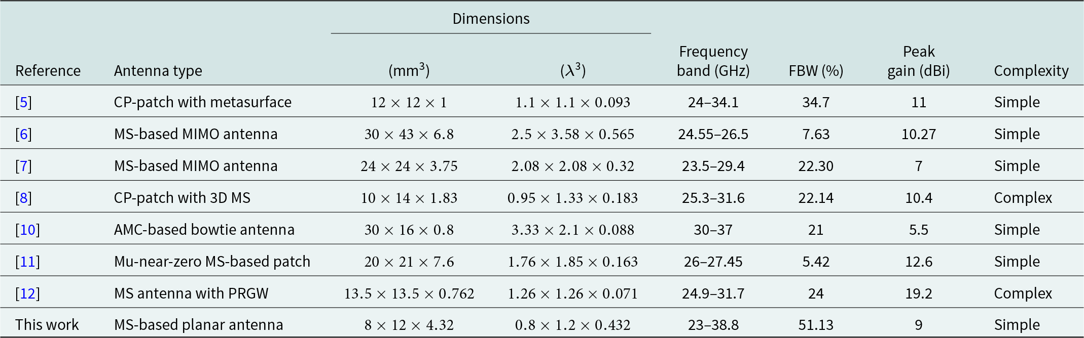
Table 2 enlists a comparison among proposed and previously presented metasurface-based antenna designs. Although the gain of the antenna is low except [Reference Sehrai, Asif, Shah, Khan, Ullah, Ibrar, Jan, Alibakhshikenari, Falcone and Limiti7, Reference Althuwayb10], it is compact compared to the designs of [Reference Tariq, Naqvi, Hussain and Amin6, Reference Sehrai, Asif, Shah, Khan, Ullah, Ibrar, Jan, Alibakhshikenari, Falcone and Limiti7, Reference Abdelaziem, Ibrahim and Abdalla11] and simple in nature compared to [Reference Ferreira-Gomes, Oliveira and Mejía-Salazar8, Reference Abdelaziem, Ibrahim and Abdalla11]. In addition, the presented antenna offers a wide impedance bandwidth and fractional bandwidth (FBW) compared to the designs listed in Table 2.
Table 2. Comparison among the proposed and previously published metasurface integrated planar antennas
Conclusion
A design of a planar wideband antenna is presented for mmWave 5G communication applications. To ensure compactness, a meander-shaped radiating element is chosen for the design. For enhanced impedance bandwidth, a partial ground plane and parasitic elements are utilized. To achieve high gain and directional radiation characteristics, a metasurface reflector is designed and placed behind the proposed planar antenna. It is observed that the designed metasurface-based antenna is able to operate well in the desired frequency band. The results show that the proposed antenna offers an impedance bandwidth of 15.8 GHz from 23 to 38.8 GHz and exhibits a peak and average gain of 9 and 6.99 dBi in the operating bandwidth, respectively. In addition, the simulated and measured performances of the proposed antenna are well in agreement. From the results, one can conclude that the proposed metasurface-based planar antenna can be a potential candidate for future 5G communication devices.
Funding statement
This research received no specific grant from any funding agency, commercial, or not-for-profit sectors.
Competing interests
The authors declare no conflict of interest.

Usman Tahir received his B.S. and M.S. degrees in Electrical Engineering from Bahria University, Islamabad, Pakistan, in 2012 and 2014. Currently, he is pursuing his Ph.D. in Electrical Engineering from the Capital University of Science and Technology, Islamabad, Pakistan. Mr. Tahir’s research interest is in antenna design for microwave and millimeter-wave (mmWave) applications.

Umair Rafique (Graduate Student Member, IEEE) received the B.S. degree in Electronic Engineering from Mohammad Ali Jinnah University (MAJU), Islamabad Campus, Karachi, Pakistan, in 2011, and the M.S. degree in Electronic Engineering from the Capital University of Science and Technology (CUST), Islamabad, Pakistan, in 2017. Currently, he is a doctoral researcher at the Center for Wireless Communication-Radio Technologies (CWC-RT), Faculty of Information Technology and Electrical Engineering, University of Oulu, Oulu, Finland. He is a recipient of the European 6G Flagship Project, where he is working toward the development of on-chip antennas and lens antennas for sub-terahertz applications. From June 2010 to January 2012, he was a research associate at the Research Group of Microelectronics and FPGAs at MAJU. From May 2013 to March 2015, he was an RF Design Engineer at AKSA Solutions Development Services (AKSA-SDS), where he was responsible for the design, development, and implementation of RF front ends for airborne and military applications. From October 2015 to May 2021, he was a research associate at the Research Group of Microelectronics and RF Engineering at CUST. He also worked as an antenna engineer with Meshtech AS, a Norway-based organization, from August 2016 to August 2017, where he was responsible for designing onboard antennas and bandpass filters for IoT applications. From February 2021 to October 2022, he worked as a researcher with the Faculty of Information Engineering, Electronics and Telecommunication at Sapienza University of Rome. He is a graduate student member of the IEEE Antennas and Propagation Society (IEEE APS), USA; the IEEE Microwave Theory and Techniques Society (IEEE MTTS), USA; and a registered engineer with the Pakistan Engineering Council (PEC). He is serving as an academic editor for Wireless Communications and Mobile Computing, Hindawi. He also acts as a referee in several highly reputed journals. He has published several research articles in reputed international journals and conferences and holds a research impact factor of 59.60 with a citation index of 475. His research interests include MIMO antennas for sub-6 GHz and mmWave applications, UWB and SWB antennas, lens antennas, frequency selective surfaces, metamaterials and metasurfaces, RF front ends and circuits, electronic system design and integration, and semiconductor device modeling.

Muhammad M. Ahmed received the Ph.D. degree in Microelectronics from the University of Cambridge, UK, in 1995 and joined academia wherein currently he is working as the Vice Chancellor of the Capital University of Science and Technology. Earlier, from 2007 to 2015, he has been the Executive Vice President of Muhammad Ali Jinnah University, Karachi, Pakistan. Through his sustained efforts, Dr. Ahmed developed and implemented a comprehensive strategy for university education and produced over 11,000 graduates at various levels to cater the needs of the society and to provide comfort to humanity. Dr. Ahmed’s research interests are in the fields of RF engineering, microelectronics, specifically in microwave devices. Numerous M.S. and Ph.D. scholars have completed their research works under his supervision. He has authored over 160 research papers, published in journals of international repute. In 2008, he was awarded a gold medal by the Pakistan Academy of Sciences for his outstanding contribution in the field of engineering and technology. Dr. Ahmed developed a comprehensive framework to simulate and model electrical characterization of field effect millimeter wave transistors both from analytical and numerical perspectives for improved understanding and CAD-related applications. He also contributed to optimization of physical parameters of microwave field effect transistors for low noise applications. In 1999, Dr. Ahmed was elected as a fellow of the Institution of Engineering and Technology (IET), UK. In the same year, he was awarded the title of Chartered Engineer (CEng) by the UK Engineering Council. He was also honored with the title of Euro Engineer (Euro Ing) in 2002 by the European Federation of National Engineering Association, Brussels. He has been the chair of a number of international conferences under the auspices of Institution of Electrical and Electronics Engineers (IEEE). Dr. Ahmed is a senior member of IEEE and holds a life membership of IEEE Electron Devices, IEEE Microwave Theory and Technique, and IEEE Antenna and Wave Propagation Societies.

Syed Muzahir Abbas (S’12-M’16-SM’18) received the B.Sc. degree in Electrical (Telecommunication) Engineering from the COMSATS Institute of Information Technology (CIIT), Islamabad, Pakistan, in 2006, the M.Sc. degree in Computer Engineering from the Center for Advanced Studies in Engineering (CASE), Islamabad, Pakistan, in 2009, and the Ph.D. degree in Electronics Engineering at Macquarie University, North Ryde, NSW, Australia, in 2016. He has been a Transmission Engineer for Alcatel-Lucent, Pakistan, RF Engineer with CommScope, Australia, and Senior Antenna Design Engineer and Senior Principal Engineer with Benelec Technologies, Australia. He has lectured various courses at CIIT, Islamabad, Pakistan, and in Australia with Western Sydney University, Macquarie University, and University of Sydney. Currently, he is working as Lead Antenna Design Engineer with GME, Australia. He has been a visiting researcher at ElectroScience Laboratory, Ohio State University, USA, and Queen Mary University of London, UK. He has also received several prestigious awards and fellowships, including 2020 IEEE 5G World Forum Best Paper Award, 2019 IEEE NSW Outstanding Young Professional Award, 2018 Young Scientist Award (Commission B – Field and Waves) from the International Union of Radio Science (URSI), 2013 CSIRO Postgraduate Fellowship, 2012 iMQRES Award for Ph.D., and Research Productivity Awards in 2012 and 2010 from CIIT, Pakistan. His research interests include base station antennas, 5G antennas, mmWave antennas, 3D printed technology, metamaterials and metasurfaces, high impedance surfaces (HIS), frequency selective surfaces (FSS), electromagnetic bandgap structures (EBG), artificial magnetic conductor (AMC), beam steering, UWB, multiband antennas, flexible/embroidered antennas, CNT yarns, CNT/graphene-based antennas, reconfigurable antennas/electronics, and the development of antennas for UWB, VHF, UHF, and WBAN applications.

Shahid Iqbal received the M.Sc. and M.Phil. degree in Electronics from Quaid-i-Azam University, Islamabad, Pakistan, in 2012 and 2015 and Ph.D. degree from State Key Laboratory of Millimeter Waves, Southeast University, Nanjing, China. He is currently working as a postdoctoral research Associate with College of Electronics and Information Engineering, Shenzhen University, Shenzhen, China. His research interest includes metamaterials, metasurfaces with multi-functional features, antennas, and waves propagation.

Sai-Wai Wong (S’06-M’09-SM’14) received the B.S degree in Electronic Engineering from the Hong Kong University of Science and Technology, Hong Kong, in 2003, and the M.Sc and Ph.D. degrees in Communication Engineering from Nanyang Technological University, Singapore, in 2006 and 2009, respectively. From July 2003 to July 2005, he was the Lead in the Engineering Department in mainland of China with two Hong Kong manufacturing companies. From 2009 to 2010, he was a Research Fellow with the Institute for Infocomm Research, Singapore. Since 2010, he was an associate professor and became a full professor with the School of Electronic and Information Engineering, South China University of Technology, Guangzhou, China. In 2016, he was a visiting Professor with the City University of Hong Kong. In 2017, he was a visiting professor with University of Macau. Since 2017, he is a tenured full professor in the College of Electronics and Information Engineering, Shenzhen University, Shenzhen, China. His current research interests include RF/microwave circuit and antenna design. Dr. Wong was a recipient of the New Century Excellent Talents in University (NCET) Award in 2013 and the Shenzhen Overseas High-Caliber Personnel Level C in 2018. He is a Reviewer for several top-tier journals.


