Mechanical properties of materials deviate from bulk behavior when characteristic dimensions become small. Such deviations may occur when either microstructural features, e.g., the grain size, or object dimensions approach the length scale of the process that controls the deformation. As a result, the mechanical strength of micro- or nanoscale pure metallic materials has been found to be an order of magnitude higher than of their bulk counterparts.[Reference Ramesh1–Reference Greer and De Hosson3] A special class of nanostructured materials are metallic nanolaminates with nanoscale layers of two different materials. They not only exhibit enhanced strength and hardness,[Reference Tsakalakos and Jankowski4–Reference Wang and Misra8] wear resistance,[Reference Ruff and Lashmore9,Reference Wen, Zong, Zeng, Gao and Pan10] or toughness,[Reference Zhang, Liu, Zhang, Zhang, Sun and Ma11] but also offer the possibility to tailor those properties by choosing material combinations.[Reference Gola, Gumbsch and Pastewka12]
Nanolaminates exhibit a range of different deformation behaviors, which depend on the combination of materials, the type of interfaces,[Reference Zhang, Li, Liang, Liu and Sun13] and the thickness of the laminate layers.[Reference Wang and Misra8] Reducing the thickness λ of the layer increases the flow strength σ of the material, with Hall–Petch-like behavior, σ ∝ λ −1/2 at large thickness transitioning to the confined layer slip σ ∝ ln(λ)/λ at smaller thickness. Shear band instabilities were observed for several crystalline systems and attributed to a reduced strain hardening ability.[Reference Wei, Jia, Ramesh and Ma14,Reference Wang, Huang, Xu, Lu and Xu15] Since shear banding is the primary failure mechanism in nanolaminates under compression,[Reference Li, Zhu, Tan, Wu, Wang and Zhang16] engineering a strong nanolaminate requires control or elimination of shear banding.
The work presented here extends on the previous investigations in two important directions: first, mechanical tests are carried out by compressing micropillars rather than through indentation. Results of pillar compression tests are easier to interpret because in contrast to indentation testing, the stress experienced by the pillar is largely uniform, and in situ observation of pillars allow a direct measurement of the deformation. Second, we present a first quantitative comparison between the experiment and accompanying molecular dynamics (MD) simulations, and the latter carried out on nanolaminate models at realistic scales and with realistic microstructures and boundary conditions.[Reference Schwaiger, Weber, Moser, Gumbsch and Kraft17] Simulations yield both mechanical properties and failure behavior of the pillars that can be directly compared with our experiments. We specifically focus on the Cu|Au nanolaminate system that has been studied extensively over the past few years.[Reference Li, Zhu, Zhang, Tan, Wang and Wu18,Reference Luo, Zhang and Schwaiger19] Cu|Au nanolaminates have a semi-coherent interface with a network of dislocations reducing the coherency stress in the layers.[Reference Shao, Wang, Beyerlein and Misra20,Reference Gola, Pastewka, Binder, Müller and Trautmann21]
Our experimental nanopillars were prepared by focused ion beam (FIB) milling from a Cu|Au nanolaminate, which had a strong Cu and Au {111} texture and had been sputter-deposited on a (100) Si substrate.[Reference Zhang, Liu, Wang and Tan22] The pillars had a taper angle of 4° and diameters at the surface and at the interface of 370 nm and 480 nm, respectively. The actual test volume was composed of a 40-layer stack of 25 nm individual thickness giving a total sample thickness of 1 µm (Fig. 1(a)). The nanopillars were compressed in situ in a scanning electron microscope (SEM, FEI Nova NanoLab 200 and Nanomechanics InSem nanoindenter) to observe their behavior during deformation.
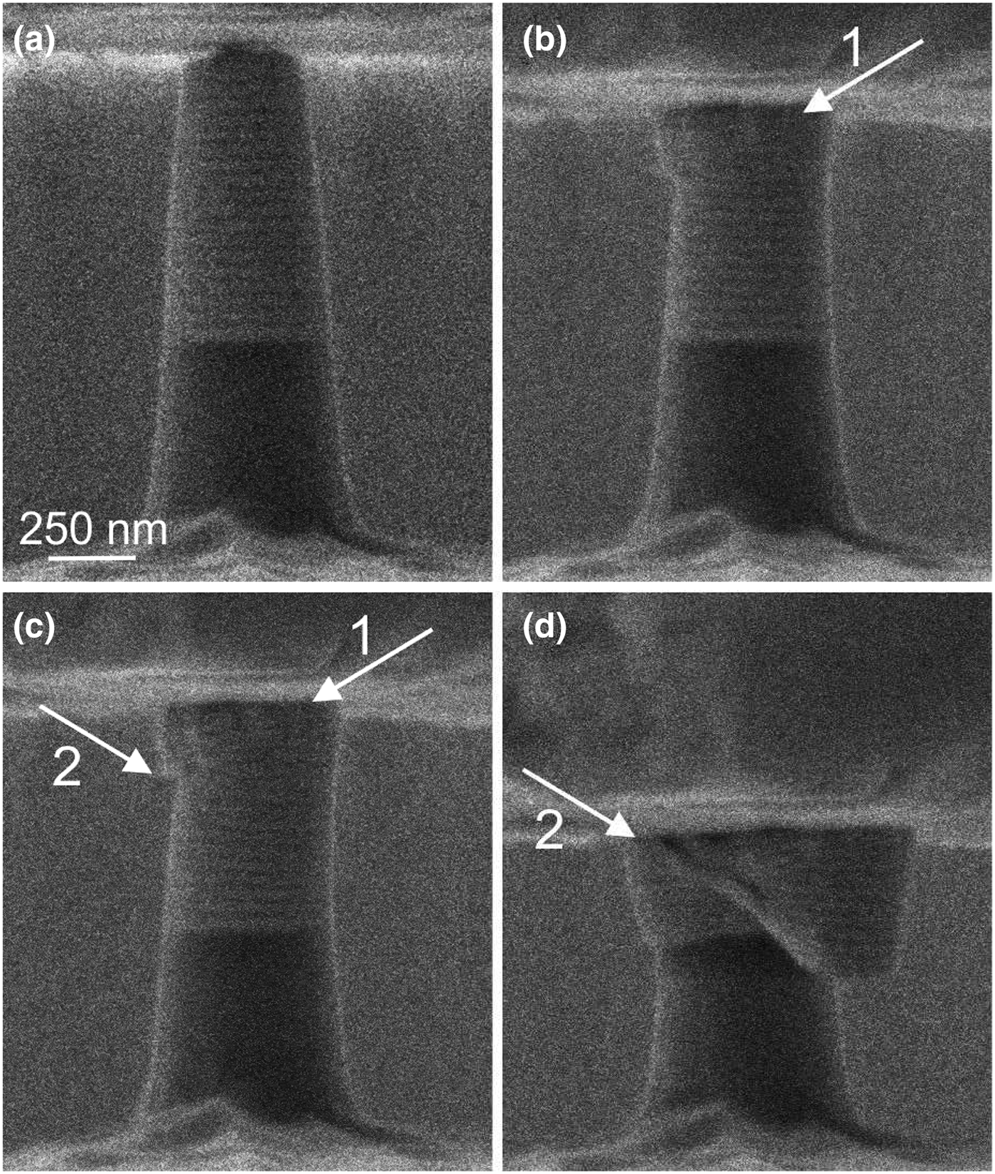
Figure 1. SEM images of deformation and failure during the compression of a nanolaminate pillar comprised of 40 layers of λ = 25 nm thickness. (a) Prior to deformation. (b) The deformation localizes at the top of the pillar and (c) forms a step on the top half (d) followed by failure through an interlayer shear band.
Figures 1(a)–1(d) show the typical outcome of such an experiment. The diamond punch first contacted the pillar on its flat top (Fig. 1(a)). Deformation then led to the gradual compression of the pillar and eventually to the nucleation of a shear band (indicated by a “1” in Figs. 1(b) and 1(c)). Shear banding localized further deformation and led to the extrusion of a wedge-shaped region near the top of the pillar. Further compression nucleated a second shear band and initiated right where the wedge had slid enough to create a surface step that concentrated stress (position “2” in Figs. 1(c) and 1(d)). Deformation then continued along this secondary shear band and eventually resulted in the failure of the pillar.
The experimental observations pose two important questions: first, it is unclear which process sets the strength of the material and which role the layer thickness plays in that process. We note that there is no evidence for slip along the interface in these pillars. Experiments on pillars with tilted interfaces and simulations on representative volume elements suggest that the interfacial shear strength is ~0.3 GPa (see Supplementary Material), but the Schmid factor for sliding along the interface for the loading geometry shown in Fig. 1 is zero. Second, homogeneous deformation was followed by the traversal of a shear band that led to the failure of the pillar. From the experiments alone, it remains unclear what conditions led to the nucleation of these shear bands. Experimental pillars often have defects from growth and FIB preparation, as, for example, surface roughness. We here hypothesize that a primary reason must be symmetry breaking due to the existence of surface flaws on either the pillar or the indenter tip.
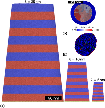
To test this hypothesis, we carried out MD calculations with varying layer thickness from 5 to 25 nm, resulting in systems of up to 380 million atoms with a total pillar height of 300 nm (Fig. 2(a)). These pillars are smaller than their experimental counterparts but have identical layer thickness and aspect ratio. The interaction between Cu and Au was modeled using a tailor-made embedded atom method potential.[Reference Gola and Pastewka23] The flat, rigid indenter was obtained by freezing the structure of a Cu50Zr50 metallic glass obtained by melting a random solid solution at 2500 K and quenching it down to 0 K at a rate of 6 K ps−1. A purely repulsive Lennard–Jones potential with interaction parameters ε Cu = 0.4093, σ Cu = 2.338, ε Au = 0.4251, σ Au = 2.485 acts between the pillar and the indenter.[Reference Halicioǧlu and Pound24] Note that the disordered nature of the indenter introduces finite friction between the indenter and the pillar. We pressed the indenter onto the pillar by displacing it at a constant applied strain rate of $\dot{\varepsilon} _{{\rm app}} = 0.8 \times 10^8\,{\rm s}^{-1}$![]() . Note that the strain-rate dependence of flow stress is negligible at these rates in FCC metals.[Reference Horstemeyer, Baskes and Plimpton25] The whole pillar was kept at 300 K using the Nosé–Hoover thermostat with a relaxation time constant of 0.5 ps. A few rows of atoms at the bottom were fixed in space to anchor the pillar to the substrate.
. Note that the strain-rate dependence of flow stress is negligible at these rates in FCC metals.[Reference Horstemeyer, Baskes and Plimpton25] The whole pillar was kept at 300 K using the Nosé–Hoover thermostat with a relaxation time constant of 0.5 ps. A few rows of atoms at the bottom were fixed in space to anchor the pillar to the substrate.
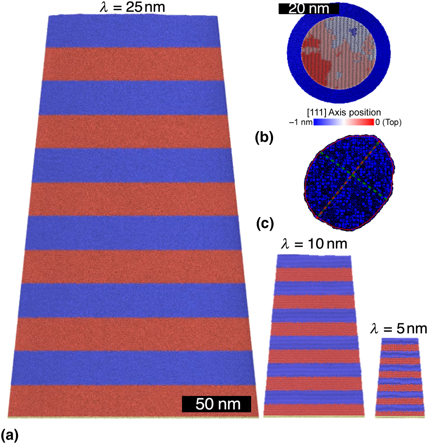
Figure 2. (a) Side view of our atomistic pillar models with layer thickness of λ = 25, 10, and 5 nm. Atoms are color-coded according to their type with Cu atoms in blue and Au atoms in red. The thin layer of yellow/gray atoms at the bottom are a rigid substrate of Au atoms. (b) Top view of the pillar model with λ = 5 nm showing a realization of random surface roughness. Atoms are colored after their position along the [111] crystallographic direction that is normal to the interfaces. (c) Cross section at one-fifth of the pillar height during compression used to compute the cross-sectional area from the MD calculations. Red- and green-dashed lines show the longest and shortest half-axes of the cross section.
We introduced different sources of defects in a controlled manner into our MD model: (i) interface defects: since Cu and Au are miscible, we intermix the interface between Cu and Au layers by randomly flipping Cu and Au atoms over a finite interface width of 15 Å, such that the final concentration profile follows the error function predicted by simple Fickian diffusion (see Ref. [Reference Gola, Pastewka, Binder, Müller and Trautmann21] for details). (ii) Surface defects: we introduced surface roughness on the pillar by cutting atoms above a plane that follows random self-affine scaling,[Reference Jacobs, Junge and Pastewka26,Reference Persson, Albohr, Tartaglino, Volokitin and Tosatti27] with a Hurst exponent of 0.8 and a root-mean-square (rms) slope of 0.1 (Fig. 2). (iii) Bulk defects: as a representative volume defect, we introduced screw dislocations at random positions and orientations.
We quantified the experiment by estimating the stress σ inside the pillar before the nucleation of the first shear band (i.e., between the states shown in Figs. 1(a) and 1(b)). To do so, we extracted the cross section d of the pillar at a position one-fifth between the top of the pillar and the Si substrate from SEM images such as those shown in Fig. 1. This gives a measure for the true strain in the pillar, ε = ln(1 + (d − d 0)/d), where d 0 is the initial diameter. Assuming rotational symmetry, it also gives an estimate of the cross-sectional area, A = πd 2/2. The stress was then obtained from indenter force F and area σ = F/A. Simulations are evaluated similarly. We computed the area A from the convex hull of the cross section at the same position along the pillar (Fig. 2(c)). Since experiments have only access to a side view and must assume rotational symmetry, we also computed the semi-minor and semi-major axes of the pillar and used their lengths to estimate the error in the determination of A (see Fig. 2(c)). Results obtained for different definitions of A (smallest and largest cross-section, exact convex hull) are indistinguishable from each other (see Supplementary Material).
Experimental data are shown by the open symbols in Fig. 3. The stress rose to a maximum of σ ~ 1.8 GPa at $\varepsilon \sim 4\%$![]() strain and then dropped during subsequent deformation. This drop is not an indication of shear softening but arises because we do not use the contacting area, but the area one-fifth from the pillar's top, to estimate the stress. Figure 3 also shows the simulated stress–strain curves for pillar models with interface and surface defects. The flow stress depends on layer thickness λ and roughly decreases with λ −1/2. Our calculation at experimental scales (λ = 25 nm) reproduces the experimental curves in the flow region, given that we introduced at least surface roughness into our system.
strain and then dropped during subsequent deformation. This drop is not an indication of shear softening but arises because we do not use the contacting area, but the area one-fifth from the pillar's top, to estimate the stress. Figure 3 also shows the simulated stress–strain curves for pillar models with interface and surface defects. The flow stress depends on layer thickness λ and roughly decreases with λ −1/2. Our calculation at experimental scales (λ = 25 nm) reproduces the experimental curves in the flow region, given that we introduced at least surface roughness into our system.
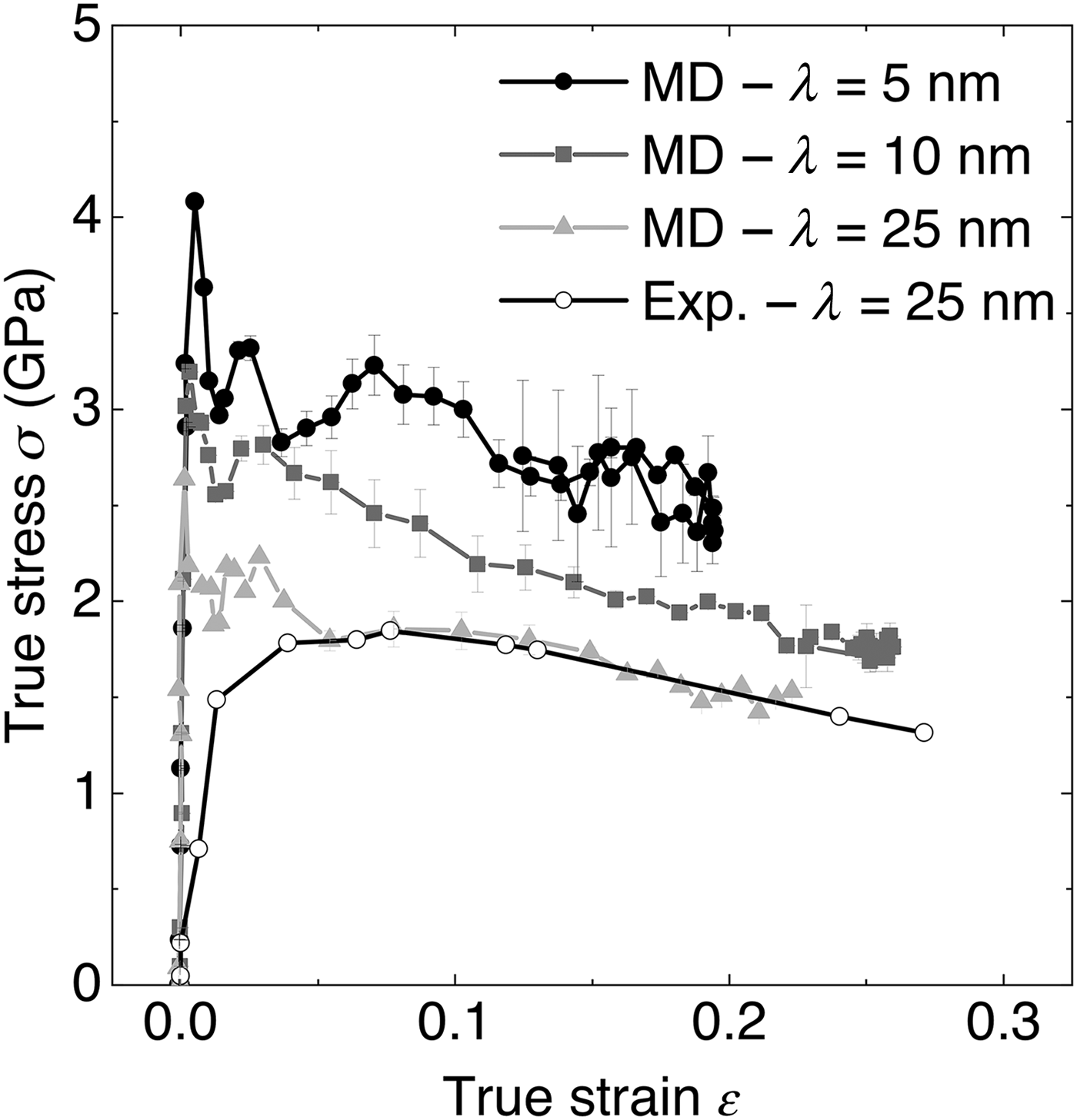
Figure 3. Stress–strain response during pillar compression obtained in experiments and through MD simulations for a different layer thickness λ. The lateral true strain and the area required to compute σ are determined from reference cross sections at one-fifth of the pillar height from the top of the pillar in all cases. The error bars of the simulated data are obtained by repeating the area measurement at distances ±1 nm of the reference cross section.
We note that experimental and simulated stress–strain curves differ at small strain where the simulations show a slight overshoot of the yield stress. This overshoot became larger as we removed defects from our system (see Supplementary Material). The nucleation of dislocations requires higher stress at lower defect density.[Reference Zepeda-Ruiz, Stukowski, Oppelstrup and Bulatov28] In addition, the nucleation of dislocations and hence the initial yield are highly strain-rate sensitive and more prominent in MD calculations because strain rates are much higher than in the experiment. Conversely, the strain-rate sensitivity is often negligible in the flow region[Reference Horstemeyer, Baskes and Plimpton25] where we find perfect agreement with the experiment.
All stress–strain curves of Fig. 3 show only the initial stages of deformation before the first shear band nucleated in experiments (Fig. 1) or simulations. Further deformation in our simulations can be classified as occurring homogeneously (Figs. 4(a) and 4(d)) or heterogeneously through the formation of a shear band (Figs. 4(b), 4(c), 4(e), and 4(f)). The formation of a shear band eventually led to a failure mode similar to the one observed experimentally (Fig. 1). A key observation in our simulations is that perfectly flat surfaces always lead to homogeneous deformation (Fig. 4(a)), while rough surfaces show heterogeneous deformation and failure (Figs. 4(b), 4(c), 4(e), and 4(f)).
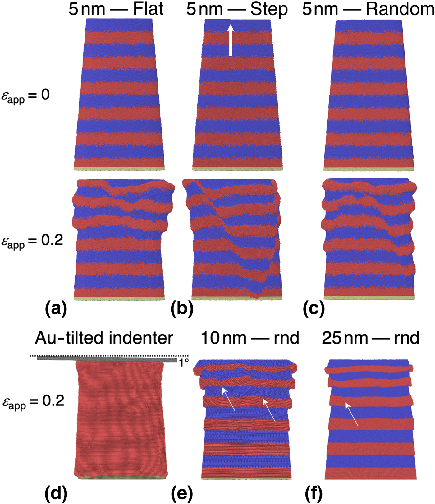
Figure 4. Comparison of the deformation mechanism for (a) an atomically flat nanopillar, (b) nanopillars with an atomic step at the surface, and (c, e, and f) nanopillars with random roughness on the top with a rms slope of 0.1. (d) Au nanopillar with a 1° tilted indenter leading to a stress concentration at the pillar edge. The top row in (a–c) corresponds to the undeformed stage of the systems, while the bottom row corresponds to the systems after the normal compressive strain of 0.2. The layer thickness ranges from 5 nm (a–c) to 10 nm (e) and 25 nm (f). The indenter has been removed for clarity for the multilayer systems. Atoms are color-coded after their type, Cu are in blue, Au are in red, and fixed atoms are in yellow. Arrow in (b) shows the initial position of the step at the surface. Arrows in (e and f) show the location of the initial formation of shear bands. Surfaces with self-affine random roughness (see text) are labelled with “rnd”.
To clarify the role played by roughness, we created pillars with the simplest model for “roughness,” a single atomic step on the surface (Fig. 4(b)). This model “roughness” already led to a deformation mechanism dramatically different from perfectly flat surfaces. A shear band is clearly visible already at an applied strain of ε app = 0.20, manifested by a series of kinks in the Cu|Au heterointerfaces and the extrusion of a wedge-shaped part of the pillar (Fig. 4(b), bottom row).
It is remarkable that the single step is sufficient to nucleate a shear band. This nucleation occurs because edges concentrate stress[Reference Johnson29] that trigger the emission of a single dislocation into the bulk. The dislocation leaves behind steps at the Cu|Au heterointerfaces, essentially imprinting the surface structure into the bulk of the material. Once a shear band has nucleated, it will accommodate all subsequent deformation since the steps or kinks created by the band themselves concentrate stress if the elastic constants differ between the layers. Figure 4(b) also shows that the individual pillar can host more than one shear band. The final snapshot of this figure clearly shows an extruded, wedge-shaped region of the pillar that is bounded by two shear bands. The deformation of the pillar is strikingly similar to the experimental result shown in Fig. 1. We were able to nucleate shear bands from steps, rough surfaces, or tilted indenters that all lead to stress concentration somewhere on the surface of the pillar.
Our explanation for the formation of the shear band relies on the existence of domains with varying elastic modulus. We therefore carried out control calculations using single-crystalline Au pillars. Those pillars deformed homogeneously even in the presence of surface steps, self-affine roughness, or a tilted indenter (Fig. 4(d) and Supplementary Material). We observed that after a dislocation nucleated at the surfaces, it subsequently traversed the full pillar, vanishing at the side walls of the pillar and leaving behind a complementary step. Unlike in nanolaminates, this dislocation does not imprint its signature into the bulk of the material. While the surface flaws are the reasons for the nucleation of an initial dislocation that constitutes the onset of the shear band, the existence of alternating sequences of hard and soft materials is the fundamental reason for its formation.[Reference Knorr, Cordero, Lilleodden and Volkert30]
In summary, we have obtained the strength of Cu|Au nanolaminate pillars from experiments and atomic-scale simulation that show excellent agreement. The strength of the pillars decreases roughly as the square root of the layer thickness down to the thinnest systems consisting of 5 nm thick layers. Our pillars localized shear in shear bands that led to a catastrophic failure of the material. We show that the nucleation process is extremely sensitive to surface flaws, but the formation of the shear band is a result of the imprinting of the surface flaws into the interface structure of the nanolaminate. Since stress concentrations in the bulk can only occur if there is a contrast between the nanolaminate layers, a possible route to suppress the shear banding instability could be the search for modulus-matched nanolaminates.
Supplementary Material
The supplementary material for this article can be found at https://doi.org/10.1557/mrc.2019.93.
Acknowledgments
We thank Peter Gumbsch for helpful discussion. This research was partially supported by the Helmholtz Association and the Chinese Academy of Sciences through a joint research group (HCJRG-217 and GJHZ1401). L.P. acknowledges funding through the Deutsche Forschungsgemeinschaft DFG (grant PA 2023/2). All MD calculations were carried out with LAMMPS.[Reference Plimpton31] ASE[Reference Hjorth Larsen, Mortensen, Blomqvist, Castelli, Christensen, Dułak, Friis, Groves, Hammer, Hargus, Hermes, Jennings, Bjerre Jensen, Kermode, Kitchin, Leonhard Kolsbjerg, Kubal, Kaasbjerg, Lysgaard, Bergmann Maronsson, Maxson, Olsen, Pastewka, Peterson, Rostgaard, Schiøtz, Schütt, Strange, Thygesen, Vegge, Vilhelmsen, Walter, Zeng and Jacobsen32] and OVITO[Reference Stukowski33] was used for pre-processing, post-processing, and visualization. Computations were carried out on NEMO (University of Freiburg, DFG grant INST 39/963-1 FUGG), ForHLR II (Steinbuch Center for Computing at the Karlsruhe Institute of Technology, project “MULTILAYER”), and JUQUEEN (Jülich Supercomputing Center, project “hka18”).


