Hostname: page-component-586b7cd67f-rcrh6 Total loading time: 0 Render date: 2024-11-30T10:52:14.806Z Has data issue: false hasContentIssue false

Automated self-assembly and electrical characterization of nanostructured films

Published online by Cambridge University Press:  02 April 2018

Rafael C. Hensel
Affiliation:
Department of Applied Physics, “Gleb Wataghin” Institute of Physics, University of Campinas––UNICAMP, 13083-970, Campinas, SP, Brazil
Kevin L. Rodrigues
Affiliation:
Department of Applied Physics, “Gleb Wataghin” Institute of Physics, University of Campinas––UNICAMP, 13083-970, Campinas, SP, Brazil
Vinicius do L. Pimentel
Affiliation:
Information Technology Center Renato Archer, 13069-901, Campinas, SP, Brazil
Antonio Riul Jr.
Affiliation:
Department of Applied Physics, “Gleb Wataghin” Institute of Physics, University of Campinas––UNICAMP, 13083-970, Campinas, SP, Brazil
Varlei Rodrigues*
Affiliation:
Department of Applied Physics, “Gleb Wataghin” Institute of Physics, University of Campinas––UNICAMP, 13083-970, Campinas, SP, Brazil
*
Address all correspondence to Varlei Rodrigues at [email protected]
Get access

Abstract

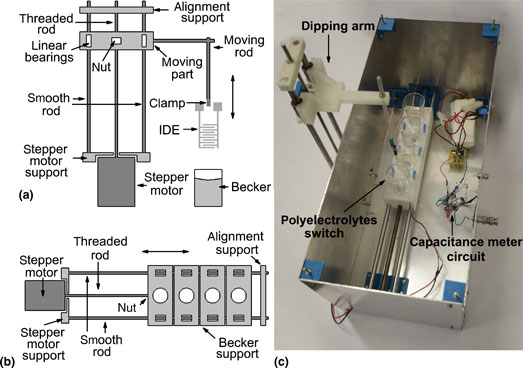
Significant progress in nanoscience was achieved through the development of methods and instruments to better comprehend nanoscale properties. We present here a methodology and automated setup to measure layer-by-layer films capacitance in the air immediately after polyelectrolytes adsorption. It presents high accuracy (~0.01 pF) to check the capacitance stabilization during spontaneous drying process in the air, with sensitivity to show electrical signal alternation accordingly to the outermost polyelectrolyte layer. Besides, a linear trend in capacitance was observed similar to UV–vis measurements. This method allows analyzing films electrical properties, affording better choice of materials, thickness, and molecular architecture.

Type
Research Letters
Copyright
Copyright © Materials Research Society 2018 

Access options

Get access to the full version of this content by using one of the access options below. (Log in options will check for institutional or personal access. Content may require purchase if you do not have access.)

References

1.Richardson, J.J., Björnmalm, M., and Caruso, F.: Technology-driven layer-by-layer assembly of nanofilms. Science 348, aaa2491 (2015).Google Scholar
2.Decher, G., Hong, J.D., and Schmitt, J.: Buildup of ultrathin multilayer films by a self-assembly process: III. Consecutively alternating adsorption of anionic and cationic polyelectrolytes on charged surfaces. Thin Solid Films 210–211, 831835 (1992).Google Scholar
3.Dey, S. and Pal, A.J.: Layer-by-layer electrostatic assembly with a control over orientation of molecules: anisotropy of electrical conductivity and dielectric properties. Langmuir 27, 86878693 (2011).Google Scholar
4.Sakai, K., Webber, G.B., Vo, C.D., Wanless, E.J., Vamvakaki, M., Bütün, V., Armes, S.P., and Biggs, S.: Characterization of layer-by-layer self-assembled multilayer films of diblock copolymer micelles. Langmuir 24, 116123 (2008).Google Scholar
5.Granholm, P., Paloheimo, J., and Stubb, H.: Charge transport in thin films of polyaniline: variable-range hopping in a parabolic quasi-gap. Phys. Status Solidi Basic Res. 205, 315318 (1998).3.0.CO;2-7>CrossRefGoogle Scholar
6.Wang, K., Cao, Y., Tagaya, M., and Kobayashi, T.: Electrochemical capacitance of poly(pyrrole-co-formylpyrrole)/sulfonated polystyrene layer-by-layer assembled multilayer films. J. Mater. Sci. 49, 57465756 (2014).CrossRefGoogle Scholar
7.Fritz, J., Cooper, E.B., Gaudet, S., Sorger, P.K., and Manalis, S.R.: Electronic detection of DNA by its intrinsic molecular charge. Proc. Natl. Acad. Sci. USA 99, 1414214146 (2002).CrossRefGoogle ScholarPubMed
8.Poghossian, A., Abouzar, M.H., Sakkari, M., Kassab, T., Han, Y., Ingebrandt, S., Offenhausser, A., and Schoning, M.J.: Field-effect sensors for monitoring the layer-by-layer adsorption of charged macromolecules. Sens. Actuators B Chem. 118, 163170 (2006).Google Scholar
9.Poghossian, A., Weil, M., Cherstvy, A.G., and Schöning, M.J.: Electrical monitoring of polyelectrolyte multilayer formation by means of capacitive field-effect devices. Anal. Bioanal. Chem. 405, 64256436 (2013).Google Scholar
10.Poghossian, A., Weil, M., and Schöning, M.: Nanoplate field-effect capacitors. In Multisensor Systems for Chemical Analysis, edited by L. Lvova, D. Kirsanov, C. Di Natale, and A. Legin (Pan Stanford Publishing, Singapore 2014), pp. 333373.Google Scholar
11.Daikuzono, C.M., Dantas, C.A.R., Volpati, D., Constantino, C.J.L., Piazzetta, M.H.O., Gobbi, A.L., Taylor, D.M., Oliveira, O.N., and Riul, A.: Microfluidic electronic tongue. Sens. Actuators B Chem. 207, 11291135 (2015).Google Scholar
12.Ladam, G., Schaad, P., Voegel, J.C., Schaaf, P., Decher, G., and Cuisinier, F.: In situ determination of the structural properties of initially deposited polyelectrolyte multilayers. Langmuir 16, 12491255, (2000).CrossRefGoogle Scholar
13.Clark, S.L. and Hammond, P.T.: Engineering the microfabrication of layer-by-layer thin films. Adv. Mater. 10, 15151519 (1998).3.0.CO;2-E>CrossRefGoogle Scholar
14.Ferreira, Q., Gomes, P.J., Maneira, M.J.P., Ribeiro, P.A., and Raposo, M.: Mechanisms of adsorption of an azo-polyelectrolyte onto layer-by-layer films. Sens. Actuators B Chem. 126, 311317 (2007).Google Scholar
15.Kern, W.: Cleaning solutions based on hydrogen peroxide for use in silicon semiconductor technology. RCA Rev. 31, 187206 (1970).Google Scholar
16.Daikuzono, C.M.: Fabricação de Filmes Ulrafinos No Interior de Microcanais. Master thesis, Universidade Federal de São Carlos, Sorocaba, 2013. https://repositorio.ufscar.br/bitstream/handle/ufscar/1171/DAIKUZONO_Cristiane_2013.pdf?sequence=1&isAllowed=yGoogle Scholar
17.Wang, X., Zheng, J., Qiao, K., Qu, J., and Cao, C.: Studies on structure and Raman spectroscopy of Ni-Doped copper phthalocyanine thin films. Appl. Surf. Sci. 297, 188194, 2014.CrossRefGoogle Scholar