Hostname: page-component-586b7cd67f-rcrh6 Total loading time: 0 Render date: 2024-11-30T12:37:38.612Z Has data issue: false hasContentIssue false

Low-temperature electrical conduction of plasma-treated bilayer MoS2

Published online by Cambridge University Press:  23 April 2018

Jakub Jadwiszczak
Affiliation:
School of Physics, Trinity College Dublin, Dublin 2, Ireland Centre for Research on Adaptive Nanostructures and Nanodevices (CRANN), Trinity College Dublin, Dublin 2, Ireland Advanced Materials and BioEngineering Research Centre (AMBER), Trinity College Dublin, Dublin 2, Ireland School of Material Science and Engineering, Nanchang University, 999 Xuefu Road, Nanchang, Jiangxi 330031, China
Yangbo Zhou
Affiliation:
School of Material Science and Engineering, Nanchang University, 999 Xuefu Road, Nanchang, Jiangxi 330031, China
Hongzhou Zhang*
Affiliation:
School of Physics, Trinity College Dublin, Dublin 2, Ireland Centre for Research on Adaptive Nanostructures and Nanodevices (CRANN), Trinity College Dublin, Dublin 2, Ireland Advanced Materials and BioEngineering Research Centre (AMBER), Trinity College Dublin, Dublin 2, Ireland
*
Address all correspondence to Hongzhou Zhang at [email protected]
Get access

Abstract

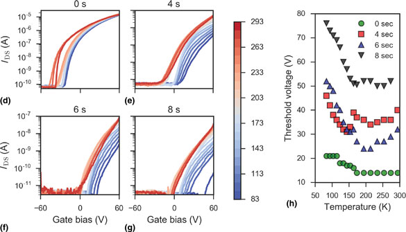
We report on the low-temperature electrical characterization of bilayer MoS2 treated with increasing dose of oxygen:argon (1:3) plasma. We characterize the effective Schottky barrier heights as a function of plasma exposure time and observe a significant barrier lowering, with no accompanying p-type conduction in the negative bias region. Furthermore, we observe a crossover in the temperature-dependent conduction regimes below 181 K due to the plasma exposure. The Efros–Shklovskii (ES) hopping regime is seen to transform upon plasma exposure to a mixed ES/thermally-activated regime at high temperatures, and to a strongly short-range Arrhenius regime at low temperatures. We attribute the observed crossovers to a critical defect density created by the surface reaction with the plasma.

Type
Research Letters
Copyright
Copyright © Materials Research Society 2018 

Access options

Get access to the full version of this content by using one of the access options below. (Log in options will check for institutional or personal access. Content may require purchase if you do not have access.)

References

1.Wang, Q.H., Kalantar-Zadeh, K., Kis, A., Coleman, J.N., and Strano, M.: Electronics and Optoelectronics of two-dimensional transition metal dichalcogenides. Nat. Nanotechnol. 7, 699712 (2012).CrossRefGoogle ScholarPubMed
2.Yu, Z., Ong, Z.-Y., Li, S., Xu, J.-B., Zhang, G., Zhang, Y.-W., Shi, Y., and Wang, X.: Analyzing the carrier mobility in transition-metal dichalcogenide MoS2 field-effect transistors. Adv. Funct. Mater. 27, 1604093 (2017).CrossRefGoogle Scholar
3.English, C.D., Shine, G., Dorgan, V.E., Saraswat, K.C., and Pop, E.: Improved contacts to MoS2 transistors by ultra-high vacuum metal deposition. Nano Lett. 16, 38243830 (2016).CrossRefGoogle ScholarPubMed
4.Chuang, S., Battaglia, C., Azcatl, A., McDonnell, S., Kang, J.S., Yin, X., Tosun, M., Kapadia, R., Fang, H., Wallace, R.M., and Javey, A.: MoS2 P-type transistors and diodes enabled by high work function MoOX contacts. Nano Lett. 14, 13371342 (2014).CrossRefGoogle ScholarPubMed
5.Chen, M., Nam, H., Wi, S., Ji, L., Ren, X., Bian, L., Lu, S., and Liang, X.: Stable few-layer MoS2 rectifying diodes formed by plasma-assisted doping. Appl. Phys. Lett. 103, 142110 (2013).CrossRefGoogle Scholar
6.Chen, M., Nam, H., Wi, S., Priessnitz, G., Gunawan, I.M., and Liang, X.: Multibit data storage states formed in plasma-treated MoS2 transistors. ACS Nano 8, 40234032 (2014).CrossRefGoogle ScholarPubMed
7.Tao, L., Duan, X., Wang, C., Duan, X., and Wang, S.: Plasma-engineered MoS2 thin-film as an efficient electrocatalyst for hydrogen evolution reaction. Chem. Commun. 51, 74707473 (2015).CrossRefGoogle ScholarPubMed
8.Giannazzo, F., Fisichella, G., Greco, G., Di Franco, S., Deretzis, I., La Magna, A., Bongiorno, C., Nicotra, G., Spinella, C., Scopelliti, M., Pignataro, B., Agnello, S., and Roccaforte, F.: Ambipolar MoS2 Transistors by nanoscale tailoring of schottky barrier using oxygen plasma functionalization. ACS Appl. Mater. Interfaces 9, 2316423174 (2017).CrossRefGoogle ScholarPubMed
9.Jadwiszczak, J., O'Callaghan, C., Zhou, Y., Fox, D.S., Weitz, E., Keane, D., Cullen, C.P., O'Reilly, I., Downing, C., Shmeliov, A., Maguire, P., Gough, J.J., McGuinness, C., Ferreira, M.S., Bradley, A.L., Boland, J.J., Duesberg, G.S., Nicolosi, V., and Zhang, H.: Oxide-mediated recovery of field-effect mobility in plasma-treated MoS2. Sci. Adv. 4, eaao5031 (2018).CrossRefGoogle ScholarPubMed
10.Jariwala, D., Sangwan, V.K., Late, D.J., Johns, J.E., Dravid, V.P., Marks, T.J., Lauhon, L.J., and Hersam, M.C.: Band-like Transport in high mobility unencapsulated single-layer MoS2 transistors. Appl. Phys. Lett. 102, 26 (2013).CrossRefGoogle Scholar
11.Baugher, B.W.H., Churchill, H.O.H., Yang, Y., and Jarillo-Herrero, P.: Intrinsic electronic transport properties of high-quality monolayer and bilayer MoS2. Nano Lett. 13, 42124216 (2013).CrossRefGoogle ScholarPubMed
12.Filanovsky, I.M. and Allam, A.: Mutual compensation of mobility and threshold voltage temperature effects with applications in CMOS circuits. IEEE Trans. Circuits Syst. I Fundam. Theory Appl. 48, 876884 (2001).CrossRefGoogle Scholar
13.Shu, J.P., Wu, G.T., Guo, Y., Liu, B., Wei, X.L., and Chen, Q.: The intrinsic origin of hysteresis in MoS2 field effect transistors. Nanoscale 8, 30493056 (2016).CrossRefGoogle ScholarPubMed
14.Khondaker, S.I. and Islam, M.R.: Bandgap engineering of MoS2 flakes via oxygen plasma: a layer dependent study. J. Phys. Chem. C 120, 1380113806 (2016).CrossRefGoogle Scholar
15.Choudhary, N., Islam, M.R., Kang, N., Tetard, L., Jung, Y., and Khondaker, S.I.: Two-dimensional lateral heterojunction through bandgap engineering of MoS2 via oxygen plasma. J. Phys. Condens. Matter. 28, 364002 (2016).CrossRefGoogle ScholarPubMed
16.Cui, N.-Y., Brown, N.M.D., and McKinley, A.: An AFM study of the topography of natural MoS2 following treatment in an RF–oxygen plasma. Appl. Surf. Sci. 151, 1728 (1999).CrossRefGoogle Scholar
17.Islam, M.R., Kang, N., Bhanu, U., Paudel, H.P., Erementchouk, M., Tetard, L., Leuenberger, M.N., and Khondaker, S.I.: Tuning the electrical property via defect engineering of single layer MoS2 by oxygen plasma. Nanoscale 6, 1003310039 (2014).CrossRefGoogle ScholarPubMed
18.Kim, C., Moon, I., Lee, D., Choi, M.S., Ahmed, F., Nam, S., Cho, Y., Shin, H., Park, S., and Yoo, W.J.: Fermi level pinning at electrical metal contacts of monolayer molybdenum dichalcogenides. ACS Nano 11, 15881596 (2017).CrossRefGoogle ScholarPubMed
19.Wang, J., Yao, Q., Huang, C., Zou, X., Liao, L., Chen, S., Fan, Z., Zhang, K., Wu, W., and Xiao, X.: High mobility MoS2 transistor with low schottky barrier contact by using atomic thick h-BN as a tunneling layer. Adv. Mater. 28, 83028308 (2016).CrossRefGoogle ScholarPubMed
20.Yildiz, A., Serin, N., Serin, T., and Kasap, M.: Crossover from nearest-neighbor hopping conduction to Efros–Shklovskii variable-range hopping conduction in hydrogenated amorphous silicon films. Jpn. J. Appl. Phys. 48, 11203 (2009).CrossRefGoogle Scholar
21.Papadopoulos, N., Steele, G.A., and van der Zant, H.S.J.: Efros-Shklovskii variable range hopping and nonlinear transport in 1 T/1 T′−MoS2. Phys. Rev. B 96, 235436 (2017).CrossRefGoogle Scholar
22.Kim, J.S., Kim, J., Zhao, J., Kim, S., Lee, J.H., Jin, Y., Choi, H., Moon, B.H., Bae, J.J., Lee, Y.H., and Lim, S.C.: Electrical transport properties of polymorphic MoS2. ACS Nano 10, 75007506 (2016).CrossRefGoogle ScholarPubMed
23.Qiu, H., Xu, T., Wang, Z., Ren, W., Nan, H., Ni, Z., Chen, Q., Yuan, S., Miao, F., Song, F., Long, G., Shi, Y., Sun, L., Wang, J., and Wang, X.: Hopping transport through defect-induced localized states in molybdenum disulphide. Nat. Commun. 4, 2642 (2013).CrossRefGoogle ScholarPubMed
24.Stanford, M.G., Pudasaini, P.R., Gallmeier, E.T., Cross, N., Liang, L., Oyedele, A., Duscher, G., Mahjouri-Samani, M., Wang, K., Xiao, K., Geohegan, D.B., Belianinov, A., Sumpter, B.G., and Rack, P.D.: High conduction hopping behavior induced in transition metal dichalcogenides by percolating defect networks: toward atomically thin circuits. Adv. Funct. Mater. 27, 1702829 (2017).CrossRefGoogle Scholar
25.Matis, B.R., Garces, N.Y., Cleveland, E.R., Houston, B.H., and Baldwin, J.W.: Electronic transport in bilayer MoS2 encapsulated in HfO2. ACS Appl. Mater. Interfaces 9, 2799528001 (2017).CrossRefGoogle ScholarPubMed
26.Efros, A.L. and Shklovskii, B.I.: Coulomb gap and low temperature conductivity of disordered systems. J. Phys. C: Solid State Phys. 8, L49 (1975).CrossRefGoogle Scholar
27.Radisavljevic, B. and Kis, A.: Mobility engineering and a metal–insulator transition in monolayer MoS2. Nat. Mater. 12, 815820 (2013).CrossRefGoogle Scholar
28.Cui, X., Lee, G.-H., Kim, Y.D., Arefe, G., Huang, P.Y., Lee, C.-H., Chenet, D.A., Zhang, X., Wang, L., Ye, F., Pizzocchero, F., Jessen, B.S., Watanabe, K., Taniguchi, T., Muller, D.A., Low, T., Kim, P., and Hone, J.: Multi-terminal transport measurements of MoS2 using a van der waals heterostructure device platform. Nat. Nanotechnol. 10, 534540 (2015).CrossRefGoogle ScholarPubMed
29.Ko, T.Y., Jeong, A., Kim, W., Lee, J., Kim, Y., Lee, J.E., Ryu, G.H., Park, K., Kim, D., Lee, Z., Lee, M.H., Lee, C., and Ryu, S.: On-stack two-dimensional conversion of MoS2 into MoO3. 2D Mater. 4, 14003 (2016).CrossRefGoogle Scholar
30.Dhall, R., Neupane, M.R., Wickramaratne, D., Mecklenburg, M., Li, Z., Moore, C., Lake, R.K., and Cronin, S.: Direct bandgap transition in many-layer MoS2 by plasma-induced layer decoupling. Adv. Mater. 27, 15731578 (2015).CrossRefGoogle ScholarPubMed
Supplementary material: File

Jadwiszczak et al. supplementary material

Figure S1

Download Jadwiszczak et al. supplementary material(File)
File 112.3 KB