Hostname: page-component-586b7cd67f-l7hp2 Total loading time: 0 Render date: 2024-11-22T21:38:04.852Z Has data issue: false hasContentIssue false

Barriers Against Copper Diffusion into Silicon and Drift Through Silicon Dioxide

Published online by Cambridge University Press:  29 November 2013

Get access

Extract

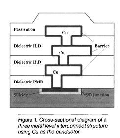
The Semiconductor Industry Association (SIA) roadmap calls for the incorporation of Cu plugs (vias) integrated with interconnects in 1997. Copper is being evaluated for ULSI metallization because of its lower bulk electrical resistivity and its superior resistance to electromigration and stress voiding as compared to commonly used aluminum and its alloys. One of the major drawbacks of Cu is its fast diffusion in Si and drift in SiO2-based dielectrics, resulting in the deterioration of devices at low temperatures. Hence a diffusion barrier is necessary between Cu and Si or SiO2. Figure 1 is a cross section of

a three metal level interconnect structure using Cu as the conductive material. The interlevel dielectrics (ILD) could be conventional SiO2-based materials or more ideally, materials with low dielectric constants such as polyimide. If conventional SiO2 is used, then Cu plugs and interconnects have to be enclosed in diffusion/drift barriers so that Cu will not move into Si or SiO2 under thermal stress or biased temperature stress (BTS).

This article reviews the published studies on conductive diffusion barriers between thin Cu films and Si substrates. In addition, the work on diffusion and drift of Cu into commonly used inorganic dielectric systems is also summarized. Finally, some concerns involving diffusion/drift barriers between Cu and Si or SiO2 for sub-0.5 μm feature size with high aspect ratios are discussed.

Type
Copper Metallization in Industry
Copyright
Copyright © Materials Research Society 1994

Access options

Get access to the full version of this content by using one of the access options below. (Log in options will check for institutional or personal access. Content may require purchase if you do not have access.)

References

1.Chang, C-A. and Hu, C-K., Appl. Phys. Lett. 57 (1990) p. 617.CrossRefGoogle Scholar
2.Dalai, H.M., Joshi, R.V., Rathore, H.S., and Fillipi, R., IEEE IEDM Technical Digest (1993) p. 273.Google Scholar
3.Lane, L.C., Nason, T.C., Yang, G-R., Lu, T-M., and Bakhru, H., J. Appl. Phys. 69 (1991) p. 6719.CrossRefGoogle Scholar
4.Reid, J.S., Chen, J.S., Kolawa, E., Nicolet, M-A., Sherman, A., and Ruiz, R., “Sputtered and CVD TiN Diffusion Barriers Between Si and Cu or Al Overlayers”, unpublished.Google Scholar
5.Olowolafe, J.O., Mogab, C.J., Gregory, R.B., and Kottke, M., J. Appl. Phys. 72 (1992) p. 4099.CrossRefGoogle Scholar
6.Choi, C.S., Ruggles, G.A., Shah, A.S., Xing, G.C., Osburn, C.M., and Hunn, J.D., J. Electrochem. Soc. 138 (1991) p. 3062; C.S. Choi, G.C. Xing, G.A. Ruggles, C.M. Osburn, A.S. Shah, and J.D. Hunn, in ULSI Science and Technology/1991, edited by J.M. Andrews and G.K. Celler (Proc. 3rd Int. Symp. on Ultra Large Scale Integration Sci. and Technol., Electrochemical Society, Pennington, New Jersey, 1991) p. 343.CrossRefGoogle Scholar
7.Awaya, N. and Arita, Y., in Digest of Technical Papers, Symposium on VLSI Technologies, Kyoto, 1989 (Business Center for Academic Society, Tokyo, 1989) p. 103.Google Scholar
8.Cho, J.S.H., Kang, H-K., Asano, I., and Wong, S.S., IEEE IEDM Technical Digest (1992) p. 297.Google Scholar
9.Cho, J.S.H., Kang, H-K., Ryu, C., and Wong, S.S., IEEE IEDM Technical Digest (1993) p. 265.Google Scholar
10.Kolawa, E., Chen, J.S., Reid, J.S., Pokela, P.J., and Nicolet, M-A., J. Appl. Phys. 70 (1991) p. 1369.CrossRefGoogle Scholar
11.Wang, S.Q., Suthar, S., Hoeflich, C., and Burrow, B.J., J. Appl. Phys. 73 (1993) p. 2301.CrossRefGoogle Scholar
12.Kolawa, E., Reid, J.S., and Chen, J-S., Submicron Metallization, Vol. 1805 (SPIE, Bellingham, WA, 1992) p. 11.Google Scholar
13.Reid, J.S., Kolawa, E., Ruiz, R.P., and Nicolet, M-A., Thin Solid Films 236 (1993) p. 319.CrossRefGoogle Scholar
14.Wang, S.Q., Raaijmakers, I.J., Burrow, B.J., Suthar, S., Redkar, S., and Kim, K-B., J. Appl. Phys. 68 (1990) p. 5176.CrossRefGoogle Scholar
15.Pokela, P.J., Kwok, C-K., Kolawa, E., Raud, S., and Nicolet, M-A., Appl. Surf. Sci. 53 (1991) p. 364.CrossRefGoogle Scholar
16.Kolawa, E., Sun, X., Reid, J.S., Chen, J.S., Nicolet, M-A., and Ruiz, R., Thin Solid Films 236 (1993) p. 301.CrossRefGoogle Scholar
17.Reid, J.S., Sun, X., Kolawa, E., and Nicolet, M-A., “Ti-Si-N Diffusion Barriers between Silicon and Copper,” IEEE Electron Device Letters, submitted.Google Scholar
18.Kolawa, E., Pokela, P.J., Reid, J.S., Chen, J.S., and Nicolet, M-A., Appl. Surf. Sci. 53 (1991) p. 373; E. Kolawa, J.S. Reid, J.S. Chen, M-A. Nicolet, and R.P. Ruiz, in Trans. 1st Int. High Temperature Electronics Conf., edited by D.B. King and F.V. Thome (Albuquerque, New Mexico, June 16–20, 1991) p. 131; E. Kolawa, P.J. Pokela, J.S. Reid, J.S. Chen, R.P. Ruiz, and M-A. Nicolet, IEEE Electron Device Lett. EDL-12 (1991) p. 321; E. Kolawa, J.S. Reid, J.S. Chen, and M-A. Nicolet, in Advanced Metallization for ULSI Application, edited by W.S. Rana, R.V. Joshi, and I. Ohdomari (Materials Research Society, Pittsburgh, PA, 1991).CrossRefGoogle Scholar
19.Kolawa, E., Pokela, P.J., Halperin, L.E., Vu, Q.T., and Nicolet, M-A., in ASM International's 3rd Electronic Materials and Processing Congress, San Francisco, CA, 1990 (ASM International, Materials Park, Ohio, 1990) p. 243.Google Scholar
20.Kolawa, E., Halperin, L.E., Pokela, P.J., Vu, Q.T., and CNieh, .W., in Advanced Metallizations in Microelectronics, edited by Katz, A., Murarka, S.P., and Appelbaum, A. (Mater. Res. Soc. Symp. Proc. 181, Pittsburgh, PA, 1990), p. 33.Google Scholar
21.Reid, J.S., Sun, X., Kolawa, E., and Nicolet, M-A., “Sputtered W-B-N Diffusion Barriers in <Si>/Cu Metallizations,” presented at ICM-CTF-94, San Diego, CA, April 25–29, 1994.Google Scholar
22.Purser, R.G., Strane, J.W., and Mayer, J.W., in Materials Reliability in Microelectronics III, edited by Rodbell, K., Filter, B., Frost, H., and Ho, P. (Mater. Res. Soc. Symp. Proc. 309, Pittsburgh, PA, 1993) p. 481.Google Scholar
23.Olowolafe, J.O., Li, J., and Mayer, J.W., J. Appl. Phys. 68 (1990) p. 6207.CrossRefGoogle Scholar
24.Chang, C-A., Appl. Phys. Lett. 55 (1989) p. 1543.CrossRefGoogle Scholar
25.Cheung, N., von Seefeld, H., and Nicolet, M-A., in Proceedings of the Symposium on Thin Film Interfaces and Interactions, edited by Baglin, J.E.E. and Poate, J.M. (The Electrochemical Society, Princeton, NJ, 1980) p. 323.Google Scholar
26.Filho, N. Mattoso, Achete, C., and Freire, F.L. Jr., Thin Solid Films 220 (1992) p. 184.CrossRefGoogle Scholar
27.Chang, C-A., J. Appl. Phys. 67 (1990) p. 6184.CrossRefGoogle Scholar
28.Ono, H., Nakano, T., and Ohta, T., Appl. Phys. Lett. 64 (1994) p. 1511; H. Ono, T. Nakano, and T. Ohta, Jpn. Soc. Appl. Phys., 40th Spring Meeting, ext. abs., March 1993, p. 812.CrossRefGoogle Scholar
29.Holloway, K. and Fryer, P.M., Appl. Phys. Lett. 57 (1990) p. 1736.CrossRefGoogle Scholar
30.Holloway, K., Fryer, P.M., Cabral, C. Jr., Harper, J.M.E., Bailey, P.J., and Kelleher, K.H., J. Appl. Phys. 71 (1992) p. 5433; K. Holloway and P.M. Fryer, in Advanced Metallizations in Microelectronics, edited by A. Katz, S.P. Murarka, and A. Appelbaum (Mater. Res. Soc. Symp. Proc. 181, Pittsburgh, PA, 1990) p. 41.CrossRefGoogle Scholar
31.Chang, C-A., J. Appl. Phys. 67 (1990) p. 7348.CrossRefGoogle Scholar
32.Catania, P., Doyle, J.P., and Cuomo, J., J. Vac. Set Technol. A 10 (1992) p. 3318.CrossRefGoogle Scholar
33.Bojarczuk, N.A., Clevenger, L.A., Holloway, K., Harper, J.M.E., Cabral, C., Schad, R.G., and Stolt, L., in Electronic Packaging Materials Science V, edited by Lillie, E.D., Ho, P.S., Jaccodine, R.J., and Jackson, K. (Mater. Res. Soc. Symp. Proc. 203, Pittsburgh, PA, 1991) p. 387.Google Scholar
34.Clevenger, L.A., Bojarczuk, N.A., Holloway, K., Harper, J.M.E., Cabral, C. Jr., Schad, R.G., and Stolt, L., J. Appl. Phys. 73 (1993) p. 300.CrossRefGoogle Scholar
35.Suni, I., Nicolet, M-A., Pai, C.S., and Lau, S.S., Thin Solid Films 107 (1983) p. 73.CrossRefGoogle Scholar
36.Wiley, J.D., Perepezko, J.H., Nordman, J.E., and Guo, K-J., Proc. Conf. on High Temperature Electronics, edited by McCormick, J.B. (IEEE, New York, 1983) p. 35; J.D. Wiley, J.H. Perepezko, J.E. Nordman, and K-J. Guo, IEEE Trans. Ind. Electron. IE-29 (2) (1982) p. 154; J.D. Wiley, J.H. Perepezko, and J.E. Nordman, Contract Report UC-63e, SAND 80-7167 (Sandia Natl. Labs., Albuquerque, NM, Dec. 1980).Google Scholar
37.Thomas, R.E., Kuo, K-J., Aaron, D.B., Dobisz, E.A., Perepezko, J.H., and Wiley, J.D., Thin Solid Films 150 (1987) p. 245.CrossRefGoogle Scholar
38. Wiley, J.D., Perepezko, J.H., and Nordman, J.E., Contract Report UC-63e, SAND 82-7156 (University of Wisconsin, Madison, WI, Sandia Contract No. 74-2536, April 1983).Google Scholar
39.de Reus, R., Koper, R.J.I.M., Zeijlemaker, H., and Saris, F.W., Mater. Lett. 9 (1990) p. 500.CrossRefGoogle Scholar
40.Yang, H., Gilmore, C.M., and Ramaker, D.E., J. Vac. Sci. Technol. A 11 (1993) p. 1454.CrossRefGoogle Scholar
41.Thomas, R.E., Perepezko, J.H., and Wiley, J.D., Appl. Surf. Sci. 26 (1986) p. 534.CrossRefGoogle Scholar
42.Reid, J.S., Kolawa, E., Stephens, T.A., Chen, J.S., and Nicolet, M-A., in Advanced Metallization for ULSI Application, edited by Rana, V.V.S., Joshi, R.V., and Ohdomari, I. (Materials Research Society, Pittsburgh, PA, 1991).Google Scholar
43.Olowolafe, J.O., Li, J., Mayer, J.W., and Colgan, E.G., Appl. Phys. Lett. 58 (1991) p. 469.CrossRefGoogle Scholar
44.Sekar, K., Satyam, P.V., Kuri, G., Mahapatra, D.P., and Dev, B.N., Nucl. Instrum. Methods Phys. Res. B 73 (1993) p. 63.CrossRefGoogle Scholar
45.Suni, I., Maenpaa, M., Nicolet, M-A., and Luomajavi, M., J. Electrochem. Soc: Solid-State Sci. Tech. 130 (1983) p. 1215.CrossRefGoogle Scholar
46.Maenpaa, M., Suni, I., Sigurd, D., Finetti, M., and Nicolet, M-A., Phys. Status Solidi A 72 (1982) p. 763.CrossRefGoogle Scholar
47.Charai, A., Hornstrom, H.E., Thomas, O., Fryer, P.M., and Harper, J.M.E., J. Vac. Sci. Technol. A7 (1989) p. 784.CrossRefGoogle Scholar
48.Li, J., Shacham-Diamand, Y., and Mayer, J.W., Mater. Sci. Rep. 9 (1992) p. 1.CrossRefGoogle Scholar
49.Poate, J.M., Tu, K.N., and Mayer, J.W., in Thin Films—Interdiffusion and Reactions (Wiley & Sons, New York, 1978) p. 376.Google Scholar
50.Ding, P.J., Lanford, W.A., Hymes, S., and Murarka, S.P., Appl. Phys. Lett. 64 (1994) p. 1.CrossRefGoogle Scholar
51.Ding, P.J., Lanford, W.A., Hymes, S., and Murarka, S.P., J. Appl. Phys. 75 (1994) p. 3627.CrossRefGoogle Scholar
52.Arcot, B., Shy, Y.T., Murarka, S.P., Shepard, C., and Lanford, W.A., in Electronic Packaging Materials Science V, edited by Lillie, E.D., Ho, P., Jaccodine, F.J., and Jackson, K. (Mater. Res. Soc. Symp. Proc. 203, Pittsburgh, PA, 1991) p. 27.Google Scholar
53.Gupta, D., Vieregge, K., and Srikrishnan, K.V., Appl. Phys. Lett. 61 (1992) p. 2178.CrossRefGoogle Scholar
54.Shacham-Diamand, Y., Dedhia, A., Hoffstetter, D., and Oldham, W.G., J. Electrochem. Soc. 140 (1993) p. 2427.CrossRefGoogle Scholar
55.McBrayer, J.D., Swanson, R.M., and Sigmon, T.W., J. Electrochem. Soc. 133 (1986) p. 1242.CrossRefGoogle Scholar
56.Nandan, R., Murarka, S.P., Pant, A., Shepard, C., and Lanford, W.A., in Advanced Metallization and Processing for Semiconductor Devices and Circuits II, edited by Katz, A., Murarka, S.P., Nissim, Y.I., and Harper, J.M.E. (Mater. Res. Soc. Symp. Proc. 260, Pittsburgh, PA, 1992) p. 929.Google Scholar
57.Murarka, S.P., Kirchner, E., Nandan, R., Eisenbraun, E., and Kaloyeros, A.E., SRC Techcon Proc. (1993) p. 381.Google Scholar
58.Kirchner, E., Murarka, S.P., Eisenbraun, E., and Kaloyeros, A.E., in Interface Control of Electrical, Chemical, and Mechanical Properties, edited by Murarka, S.P., Rose, K., Ohmi, T., and Seidel, T. (Mater. Res. Soc. Symp. Proc. 318, Pittsburgh, PA, 1994) p. 319.Google Scholar
59.Berti, A., Murarka, S.P., Ding, P.J., and Lanford, W.A., “Titanium Nitride as an Adhesion and Diffusion Barrier for Copper,” NY SCOE Review (Rensselaer Polytechnic Institute and State University of New York at Albany, Troy, NY, Nov. 9–10, 1993).Google Scholar
60.Smy, T., Westra, K.L., and Brett, M.J., IEEE Trans. Electron Devices 37 (1990) p. 591.CrossRefGoogle Scholar
61.Tail, R.N., Dew, S.K., Smy, T., and Brett, M.J., J. Appl. Phys. 70 (1991) p. 4295.Google Scholar
62.Rogers, B.R., in Advanced Metallization for ULSI Applications 1992, edited by Cale, T.S. and Pintchovski, F.S. (Materials Research Society, Pittsburgh, PA, 1993) p. 341.Google Scholar
63.Joshi, R.V., Dibello, G.W., Cuomo, J.J., Domenicucci, A.G., and Singh, R.P., in Advanced Metallization for ULSI Applications 1992, edited by Cale, T.S. and Pintchovski, F.S. (Materials Research Society, Pittsburgh, PA, 1993), p. 273.Google Scholar
64.Hsieh, J.J. and Joshi, R.V., in Advanced Metallization for ULSI Applications 1993, edited by Favreau, D.P., Shacham-Diamand, Y., and Horiike, Y. (Materials Research Society, Pittsburgh, PA, 1994) p. 207.Google Scholar