Hostname: page-component-586b7cd67f-rcrh6 Total loading time: 0 Render date: 2024-11-26T19:12:01.608Z Has data issue: false hasContentIssue false

Effects of tunneling-based access resistance in layered single-crystalline organic transistors

Published online by Cambridge University Press:  11 July 2018

Takamasa Hamai*
Affiliation:
Department of Applied Physics, The University of Tokyo, Tokyo 113-8656, Japan
Shunto Arai
Affiliation:
Department of Applied Physics, The University of Tokyo, Tokyo 113-8656, Japan
Tatsuo Hasegawa
Affiliation:
Department of Applied Physics, The University of Tokyo, Tokyo 113-8656, Japan; and Flexible Electronics Research Center, National Institute of Advanced Industrial Science and Technology (AIST), Tsukuba 305-8565, Japan
*
a)Address all correspondence to this author. e-mail: [email protected]
Get access

Abstract

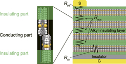
7-Decyl-2-phenyl[1]benzothieno[3,2-b][1]benzothiophene (Ph-BTBT-C10) is a soluble organic semiconductor that can afford high mobility organic thin-film transistors (OTFTs). The material exhibits inherent high layered crystallinity due to the formation of bilayer-type layered-herringbone packing that involves nearly independent π-electron core layers and alkyl-chain layers within the crystals. Here, we discuss that the bottom-gate/top-contact OTFTs composed of single-crystalline Ph-BTBT-C10 channel layers exhibit noticeable effects in the device characteristics caused by the highly insulating nature of the alkyl-chain layers. Notable layer-number (n) dependence was observed in the nonlinear current–voltage characteristics and the device mobility (2–14 cm2/Vs, with TFT ideality factor 15–46%, mainly due to large threshold voltages), which can be clearly ascribed to the tunneling-based interlayer access resistance across the alkyl-chain layers. The gated-four-probe measurements of single-crystalline OTFTs also revealed quite high mobility more than 40 cm2/Vs along the channel semiconducting layer, whereas highly insulating effects due to the alkyl-chain layers were also apparent as the large hysteresis in the gate-off states of OTFTs. We discuss the whole features of the tunneling-based access resistance in the device operations of single-crystalline OTFTs, on the basis of comparison between experimental results and model simulations.

Type
Invited Paper
Copyright
Copyright © Materials Research Society 2018 

Access options

Get access to the full version of this content by using one of the access options below. (Log in options will check for institutional or personal access. Content may require purchase if you do not have access.)

References

REFERENCES

Sirringhaus, H.: 25th anniversary article: Organic field-effect transistors: The path beyond amorphous silicon. Adv. Mater. 26, 1319 (2014).CrossRefGoogle ScholarPubMed
Mei, J., Diao, Y., Appleton, A.L., Fang, L., and Bao, Z.: Integrated materials design of organic semiconductors for field-effect transistors. J. Am. Chem. Soc. 135, 6724 (2013).CrossRefGoogle ScholarPubMed
Kang, B., Lee, W.H., and Cho, K.: Recent advances in organic transistor printing processes. ACS Appl. Mater. Interfaces 5, 2302 (2013).CrossRefGoogle ScholarPubMed
Ebata, H., Izawa, T., Miyazaki, E., Takimiya, K., Ikeda, M., Kuwabara, H., and Yui, T.: Highly soluble [1]benzothieno[3,2-b]benzothiophene (BTBT) derivatives for high-performance, solution-processed organic field-effect transistors. J. Am. Chem. Soc. 129, 15732 (2007).CrossRefGoogle ScholarPubMed
Mitsui, C., Okamoto, T., Yamagishi, M., Tsurumi, J., Yoshimoto, K., Nakahara, K., Soeda, J., Hirose, Y., Sato, H., Yamano, A., Uemura, T., and Takeya, J.: High-performance solution-processable N-shaped organic semiconducting materials with stabilized crystal phase. Adv. Mater. 26, 4546 (2014).CrossRefGoogle ScholarPubMed
Inoue, S., Minemawari, H., Tsutsumi, J., Chikamatsu, M., Yamada, T., Horiuchi, S., Tanaka, M., Kumai, R., Yoneya, M., and Hasegawa, T.: Effects of substituted alkyl chain length on solution-processable layered organic semiconductor crystals. Chem. Mater. 27, 3809 (2015).CrossRefGoogle Scholar
Minemawari, H., Tanaka, M., Tsuzuki, S., Inoue, S., Yamada, T., Kumai, R., Shimoi, Y., and Hasegawa, T.: Enhanced layered-herringbone packing due to long alkyl chain substitution in solution-processable organic semiconductors. Chem. Mater. 29, 1245 (2017).CrossRefGoogle Scholar
Tsutsumi, J., Matsuoka, S., Inoue, S., Minemawari, H., Yamada, T., and Hasegawa, T.: N-type field-effect transistors based on layered crystalline donor–acceptor semiconductors with dialkylated benzothienobenzothiophenes as electron donors. J. Mater. Chem. C 3, 1976 (2015).CrossRefGoogle Scholar
Shibata, Y., Tsutsumi, J., Matsuoka, S., Minemawari, H., Arai, S., Kumai, R., and Hasegawa, T.: Unidirectionally crystallized stable n-type organic thin-film transistors based on solution-processable donor-acceptor compounds. Adv. Electron. Mater. 3, 1700097 (2017).CrossRefGoogle Scholar
McCulloch, I., Heeney, M., Bailey, C., Genevicius, K., Macdonald, I., Shkunov, M., Sparrowe, D., Tierney, S., Wagner, R., Zhang, W., Chabinyc, M.L., Kline, R.J., McGehee, M.D., and Toney, M.F.: Liquid-crystalline semiconducting polymers with high charge-carrier mobility. Nat. Mater. 5, 328 (2006).CrossRefGoogle ScholarPubMed
Minemawari, H., Tsutsumi, J., Inoue, S., Yamada, T., Kumai, R., and Hasegawa, T.: Crystal structure of asymmetric organic semiconductor 7-decyl-2-phenyl[1]benzothieno[3,2-b][1]benzothiophene. Appl. Phys. Express 7, 91601 (2014).CrossRefGoogle Scholar
Minemawari, H., Yamada, T., Matsui, H., Tsutsumi, J., Haas, S., Chiba, R., Kumai, R., and Hasegawa, T.: Inkjet printing of single-crystal films. Nature 475, 364 (2011).CrossRefGoogle ScholarPubMed
Uemura, T., Nakayama, K., Hirose, Y., Soeda, J., Uno, M., Li, W., Yamagishi, M., Okada, Y., and Takeya, J.: Band-like transport in solution-crystallized organic transistors. Curr. Appl. Phys. 12, S87 (2012).CrossRefGoogle Scholar
Soeda, J., Uemura, T., Okamoto, T., Mitsui, C., Yamagishi, M., and Takeya, J.: Inch-size solution-processed single-crystalline films of high-mobility organic semiconductors. Appl. Phys. Express 6, 76503 (2013).CrossRefGoogle Scholar
Iino, H., Usui, T., and Hanna, J.: Liquid crystals for organic thin-film transistors. Nat. Commun. 6, 6828 (2015).CrossRefGoogle ScholarPubMed
Soeda, J., Okamoto, T., Mitsui, C., and Takeya, J.: Stable growth of large-area single crystalline thin films from an organic semiconductor/polymer blend solution for high-mobility organic field-effect transistors. Org. Electron. 39, 127 (2016).CrossRefGoogle Scholar
Peng, B., Huang, S., Zhou, Z., and Chan, P.K.L.: Solution-processed monolayer organic crystals for high-performance field-effect transistors and ultrasensitive gas sensors. Adv. Funct. Mater. 27, 1700999 (2017).CrossRefGoogle Scholar
Diao, Y., Tee, B.C-K., Giri, G., Xu, J., Kim, D.H., Becerril, H.A., Stoltenberg, R.M., Lee, T.H., Xue, G., Mannsfeld, S.C.B., and Bao, Z.: Solution coating of large-area organic semiconductor thin films with aligned single-crystalline domains. Nat. Mater. 12, 665 (2013).CrossRefGoogle ScholarPubMed
Janneck, R., Vercesi, F., Heremans, P., Genoe, J., and Rolin, C.: Predictive model for the meniscus-guided coating of high-quality organic single-crystalline thin films. Adv. Mater. 28, 8007 (2016).CrossRefGoogle ScholarPubMed
Hamai, T., Arai, S., Minemawari, H., Inoue, S., Kumai, R., and Hasegawa, T.: Tunneling and origin of large access resistance in layered-crystal organic transistors. Appl. Phys. Rev. 8, 54011 (2017).CrossRefGoogle Scholar
Dürr, A.C., Schreiber, F., Kelsch, M., Carstanjen, H.D., Dosch, H., and Seeck, O.H.: Morphology and interdiffusion behavior of evaporated metal films on crystalline diindenoperylene thin films. J. Appl. Phys. 93, 5201 (2003).CrossRefGoogle Scholar
Xu, Y., Liu, C., Sun, H., Balestra, F., Ghibaudo, G., Scheideler, W., and Noh, Y.Y.: Metal evaporation dependent charge injection in organic transistors. Org. Electron. 15, 1738 (2014).CrossRefGoogle Scholar
Podzorov, V., Sysoev, S.E., Loginova, E., Pudalov, V.M., and Gershenson, M.E.: Single-crystal organic field effect transistors with the hole mobility ∼8 cm2/V s. Appl. Phys. Lett. 83, 3504 (2003).CrossRefGoogle Scholar
Gundlach, D.J., Zhou, L., Nichols, J.A., Jackson, T.N., Necliudov, P.V., and Shur, M.S.: An experimental study of contact effects in organic thin film transistors. J. Appl. Phys. 100, 24509 (2006).CrossRefGoogle Scholar
Minari, T., Miyadera, T., Tsukagoshi, K., Aoyagi, Y., and Ito, H.: Charge injection process in organic field-effect transistors. Appl. Phys. Lett. 91, 053508 (2007).CrossRefGoogle Scholar
Wang, S.D., Minari, T., Miyadera, T., Tsukagoshi, K., and Aoyagi, Y.: Contact-metal dependent current injection in pentacene thin-film transistors. Appl. Phys. Lett. 91, 203508 (2007).CrossRefGoogle Scholar
Minari, T., Darmawan, P., Liu, C., Li, Y., Xu, Y., and Tsukagoshi, K.: Highly enhanced charge injection in thienoacene-based organic field-effect transistors with chemically doped contact. Appl. Phys. Lett. 100, 093303 (2012).CrossRefGoogle Scholar
Choi, H.H., Cho, K., Frisbie, C.D., Sirringhaus, H., and Podzorov, V.: Critical assessment of charge mobility extraction in FETs. Nat. Mater. 17, 2 (2018).CrossRefGoogle Scholar
Torricelli, F., Ghittorelli, M., Colalongo, L., and Kovacs-Vajna, Z.M.: Single-transistor method for the extraction of the contact and channel resistances in organic field-effect transistors. Appl. Phys. Lett. 104, 93303 (2014).CrossRefGoogle Scholar
Yamagishi, Y., Noda, K., Kobayashi, K., and Yamada, H.: Interlayer resistance and edge-specific charging in layered molecular crystals revealed by Kelvin-probe force microscopy. J. Phys. Chem. C 119, 3006 (2015).CrossRefGoogle Scholar
Takagi, S., Koga, J., and Toriumi, A.: Subband structure engineering for performance enhancement of Si MOSFETs. Int. Electron Devices Meet. IEDM Tech. Dig. 410, 219 (1997).CrossRefGoogle Scholar
Podzorov, V., Pudalov, V.M., and Gershenson, M.E.: Field-effect transistors on rubrene single crystals with parylene gate insulator. Appl. Phys. Lett. 82, 1739 (2003).CrossRefGoogle Scholar
Pesavento, P.V., Chesterfield, R.J., Newman, C.R., and Frisble, C.D.: Gated four-probe measurements on pentacene thin-film transistors: Contact resistance as a function of gate voltage and temperature. J. Appl. Phys. 96, 7312 (2004).CrossRefGoogle Scholar
Pesavento, P.V., Puntambekar, K.P., Frisbie, C.D., McKeen, J.C., and Ruden, P.P.: Film and contact resistance in pentacene thin-film transistors: Dependence on film thickness, electrode geometry, and correlation with hole mobility. J. Appl. Phys. 99, 94504 (2006).CrossRefGoogle Scholar
Takeya, J., Yamagishi, M., Tominari, Y., Hirahara, R., Nakazawa, Y., Nishikawa, T., Kawase, T., Shimoda, T., and Ogawa, S.: Very high-mobility organic single-crystal transistors with in-crystal conduction channels. Appl. Phys. Lett. 90, 102120 (2007).CrossRefGoogle Scholar
Uemura, T., Rolin, C., Ke, T-H., Fesenko, P., Genoe, J., Heremans, P., and Takeya, J.: On the extraction of charge carrier mobility in high-mobility organic transistors. Adv. Mater. 28, 151 (2016).CrossRefGoogle ScholarPubMed
Yi, H.T., Chen, Y., Czelen, K., and Podzorov, V.: Vacuum lamination approach to fabrication of high-performance single-crystal organic field-effect transistors. Adv. Mater. 23, 5807 (2011).CrossRefGoogle ScholarPubMed
Bittle, E.G., Basham, J.I., Jackson, T.N., and Jurchescu, O.D.: Mobility overestimation due to gated contacts in organic field-effect transistors. Nat. Commun. 7, 10908 (2016).CrossRefGoogle ScholarPubMed
Moscatello, J.P., Castaneda, C.V., Zaidi, A., Cao, M., Usluer, O., Briseno, A.L., and Aidala, K.E.: Time-resolved kelvin probe force microscopy to study population and depopulation of traps in electron or hole majority organic semiconductors. Org. Electron. 41, 26 (2017).CrossRefGoogle Scholar
Simmons, J.G.: Generalized formula for the electric tunnel effect between similar electrodes separated by a thin insulating film. J. Appl. Phys. 34, 1793 (1963).CrossRefGoogle Scholar
Wang, W., Lee, T., and Reed, M.A.: Mechanism of electron conduction in self-assembled alkanethiol monolayer devices. Phys. Rev. B 68, 35416 (2003).CrossRefGoogle Scholar
Lee, T., Wang, W., Klemic, J.F., Zhang, J.J., Su, J., and Reed, M.A.: Comparison of electronic transport characterization methods for alkanethiol self-assembled monolayers. J. Phys. Chem. B 108, 8742 (2004).CrossRefGoogle Scholar
Salomon, A., Boecking, T., Chan, C.K., Amy, F., Girshevitz, O., Cahen, D., and Kahn, A.: How do electronic carriers cross Si-bound alkyl monolayers? Phys. Rev. Lett. 95, 266807 (2005).CrossRefGoogle ScholarPubMed
Salomon, A., Shpaisman, H., Seitz, O., Boecking, T., and Cahen, D.: Temperature-dependent electronic transport through alkyl chain monolayers: Evidence for a molecular signature. J. Phys. Chem. C 112, 3969 (2008).CrossRefGoogle Scholar
Richards, T.J. and Sirringhaus, H.: Analysis of the contact resistance in staggered, top-gate organic field-effect transistors. J. Appl. Phys. 102, 94510 (2007).CrossRefGoogle Scholar