Skip to main content Accessibility help
×
Hostname: page-component-78c5997874-j824f Total loading time: 0 Render date: 2024-11-05T12:52:11.772Z Has data issue: true hasContentIssue false

References

Published online by Cambridge University Press:  24 February 2018

Farzan Jazaeri
Affiliation:
École Polytechnique Fédérale de Lausanne
Jean-Michel Sallese
Affiliation:
École Polytechnique Fédérale de Lausanne
Get access

Summary

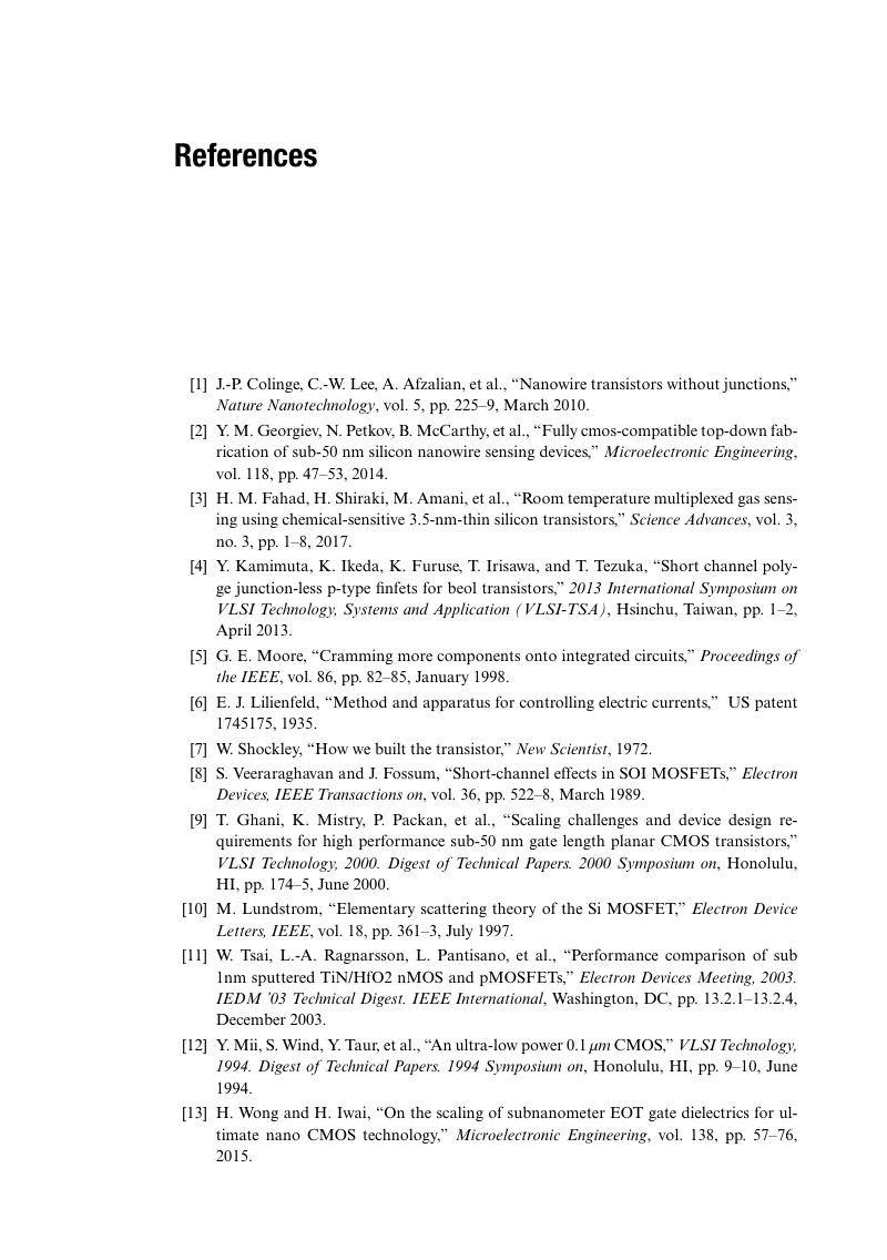
Image of the first page of this content. For PDF version, please use the ‘Save PDF’ preceeding this image.'
Type
Chapter
Information
Publisher: Cambridge University Press
Print publication year: 2018

Access options

Get access to the full version of this content by using one of the access options below. (Log in options will check for institutional or personal access. Content may require purchase if you do not have access.)

References

[1] J.-P., Colinge, C.-W., Lee, A., Afzalian, et al., “Nanowire transistors without junctions,Nature Nanotechnology, vol. 5, pp. 225–9, March 2010.
[2] Y.M., Georgiev, N., Petkov, B., McCarthy, et al., “Fully cmos-compatible top-down fabrication of sub-50 nm silicon nanowire sensing devices,Microelectronic Engineering, vol. 118, pp. 47–53, 2014.
[3] H.M., Fahad, H., Shiraki, M., Amani, et al., “Room temperature multiplexed gas sensing using chemical-sensitive 3.5-nm-thin silicon transistors,Science Advances, vol. 3, no. 3, pp. 1–8, 2017.
[4] Y., Kamimuta, K., Ikeda, K., Furuse, T., Irisawa, and T., Tezuka, “Short channel polyge junction-less p-type finfets for beol transistors,” 2013 International Symposium on VLSI Technology, Systems and Application (VLSI-TSA), Hsinchu, Taiwan, pp. 1–2, April 2013.
[5] G.E., Moore, “Cramming more components onto integrated circuits,Proceedings of the IEEE, vol. 86, pp. 82–85, January 1998.
[6] E.J., Lilienfeld, “Method and apparatus for controlling electric currents,” US patent 1745175, 1935.
[7] W., Shockley, “How we built the transistor,” New Scientist, 1972.
[8] S., Veeraraghavan and J., Fossum, “Short-channel effects in SOI MOSFETs,Electron Devices, IEEE Transactions on, vol. 36, pp. 522–8, March 1989.
[9] T., Ghani, K., Mistry, P., Packan, et al., “Scaling challenges and device design requirements for high performance sub-50 nm gate length planar CMOS transistors,” VLSI Technology, 2000. Digest of Technical Papers. 2000 Symposium on, Honolulu, HI, pp. 174–5, June 2000.
[10] M., Lundstrom, “Elementary scattering theory of the Si MOSFET,Electron Device Letters, IEEE, vol. 18, pp. 361–3, July 1997.
[11] W., Tsai, L.-A., Ragnarsson, L., Pantisano, et al., “Performance comparison of sub 1nm sputtered TiN/HfO2 nMOS and pMOSFETs,” Electron Devices Meeting, 2003. IEDM ‘03 Technical Digest. IEEE International, Washington, DC, pp. 13.2.1–13.2.4, December 2003.
[12] Y., Mii, S., Wind, Y., Taur, et al., “An ultra-low power 0:1 _m CMOS,” VLSI Technology, 1994. Digest of Technical Papers. 1994 Symposium on, Honolulu, HI, pp. 9–10, June 1994.
[13] H., Wong and H., Iwai, “On the scaling of subnanometer EOT gate dielectrics for ultimate nano CMOS technology,Microelectronic Engineering, vol. 138, pp. 57–76, 2015.
[14] A., Chatterjee, R., Chapman, K., Joyner, et al., “CMOS metal replacement gate transistors using tantalum pentoxide gate insulator,” Electron Devices Meeting, 1998. IEDM '98. Technical Digest., International, San Francisco, CA, pp. 777–80, December 1998.
[15] D., Frank, S., Laux, and M., Fischetti, “Monte Carlo simulation of a 30 nm dual-gate MOSFET: how short can Si go?,” Electron Devices Meeting, 1992. IEDM ‘92. Technical Digest., International, San Francisco, CA, pp. 553–6, December 1992.
[16] K., Ismail, “Si/SiGe high-speed field-effect transistors,” in Electron Devices Meeting, 1995. IEDM ‘95, International, pp. 509–12, December 1995.
[17] W.P., Maly, “Integrated circuit device, system, and method of fabrication,” US patent WO2007133775A2, May 2012.
[18] W., Maly, “Vertical slit transistor based integrated circuits (VeSTICs) paradigm,” ISPD, pp. 63–4, 2009.
[19] W., Maly, N., Singh, Z., Chen, and N., Shen, “Twin gate, vertical slit FET (VeSFET) for highly periodic layout and 3D integration,” Proceedings of the 18th International Conference Mixed Design of Integrated Circuits and Systems – MIXDES 2011, Gliwice, pp. 145–50, 2011.
[20] H., Lu and A., Seabaugh, “Tunnel field-effect transistors: State-of-the-art,IEEE Journal of the Electron Devices Society, vol. 2, pp. 44–9, July 2014.
[21] J., Welser, S., Tiwari, S., Rishton, K., Lee, and Y., Lee, “Room temperature operation of a quantum-dot flash memory,Electron Device Letters, IEEE, vol. 18, pp. 278–80, June 1997.
[22] A., Pfitzner, M., Staniewski, and M., Strzyga, “DC characteristics of junction vertical slit field-effect transistor (JVeSFET),” 2009 MIXDES-16th International Conference Mixed Design of Integrated Circuits & Systems, Lodz, pp. 420–3, June 2009.
[23] X., Qiu, M., Marek-Sadowska, and W., Maly, “Vertical slit field effect transistor in ultralow power applications,” Quality Electronic Design (ISQED), 2012 13th International Symposium on, Santa Clara, CA, pp. 384–90, March 2012.
[24] N., Sugii, “Low-power-consumption fully depleted silicon-on-insulator technology,Microelectronic Engineering, vol. 132, pp. 226–35, 2015.
[25] S., Zhu, J., Chen, M.-F., Li, et al., “ N-type Schottky barrier source/drain MOSFET using Ytterbium silicide,IEEE Electron Devices Letters, vol. 25, pp. 565–7, April 2004.
[26] M.K., Ieong, P.M., Solomon, S.E., Laux, H.-S., Philip Wong, and D., Chidambarrao, “Comparison of raised and Schottky source/drain MOSFETs using a novel tunneling contact model,” Electron Devices Meeting, 1998. IEDM ‘98. Technical Digest., International, San Francisco, CA, pp. 733–8, December 1998.
[27] C.-W., Lee, I., Ferain, A., Afzalian, et al., “Performance estimation of junctionless multigate transistors,Solid-State Electronics, vol. 54, pp. 97–103, February 2010.
[28] C.-W., Lee, A., Afzalian, N.D., Akhavan, et al., “Junctionless multigate field effect transistor,Applied Physical Letters, vol. 94, pp. 053511-1–053511-2, February 2009.
[29] J.P., Colinge, C.W., Lee, A., Afzalian, et al., “SOI gated resistor: CMOS without junctions,” IEEE International SOI Conference, Foster City, CA, pp. 1–2, October 2009.
[30] M.-H., Han, C.-Y., Chang, H.-B., Chen, Y.-C., Cheng, and Y.-C., Wu, “Device and circuit performance estimation of junctionless bulk FinFETs,Electron Devices, IEEE Transactions on, vol. 60, pp. 1807–13, June 2013.
[31] M.-H., Han, C.-Y., Chang, H.-B., Chen, et al., “Performance comparison between bulk and SOI junctionless transistors,Electron Device Letters, IEEE, vol. 34, pp. 169–71, February 2013.
[32] Z., Chen, A., Kamath, N., Singh, et al., “ N-channel junctionless vertical slit field effect transistor (VeSFET): fabrication-based feasibility assessment,International Conference on Solid-State and Integrated Circuit (ICSIC 2012), Singapore, vol. 32, pp. 152–4, 2012.
[33] A., Kamath, Z., Chen, N., Shen, et al., “Realizing and and or functions with single vertical-slit field effect transistor,IEEE Electron Device Letters, vol. 33, pp. 152–4, February 2012.
[34] V., Nandakumar and M., Marek-Sadowska, “A low energy network-on-chip fabric for 3-D multi-core architectures,Emerging and Selected Topics in Circuits and Systems, IEEE Journal on, vol. 2, pp. 266–77, June 2012.
[35] M., Pastre, F., Krummenacher, L., Barbut, J.-M., Sallese, and M., Kayal, “Towards circuit design using VeSFETs,” Mixed Design of Integrated Circuits and Systems (MIXDES), 2011 Proceedings of the 18th International Conference, Gliwice, Poland, pp. 139–44, June 2011.
[36] M., Weis, A., Pfitzner, K., Kasprowicz, et al., “Low power SRAM cell using vertical slit field effect transistor (VeSFET),” European Solid-State Circuits Conference ESSCIRC Fringe, Edinburgh, UK, 2008.
[37] E., Gnani, A., Gnudi, S., Reggiani, et al., “Numerical investigation on the junctionless nanowire FET,” IEEE Ultimate Integration on Silicon (ULIS) Conference, Cork, Ireland, pp. 1–4, March 2011.
[38] R., Rios, A., Cappellani, M., Armstrong, et al., “Comparison of junctionless and conventional trigate transistors with Lg down to 26 nm,IEEE Transaction Electron Devices, vol. 32, pp. 1170–2, September 2011.
[39] W., Vitale, M., Mohamed, and U., Ravaioli, “Monte Carlo study of transport properties in junctionless transistors,” 2010 14th International Workshop on Computational Electronics, Pisa, pp. 1–3, October 2010.
[40] H.-C., Lin, C.-I., Lin, and T.-Y., Huang, “Characteristics of n-type junctionless poly-Si thin-film transistors with an ultrathin channel,IEEE Electron Device letters, vol. 33, pp. 53–5, January 2012.
[41] P., Razavi, G., Fagas, I., Ferain, et al., “Performance investigation of short-channel junctionless multigate transistors,” IEEE Ultimate Integration on Silicon (ULIS), pp. 1–4, March 2011.
[42] P., Francis, A., Terao, D., Flandre, and F., Van de Wiele, “Moderate inversion model of ultrathin double-gate nMOS/SOI transistors,Solid State Electronics, vol. 38, pp. 171– 6, March 1995.
[43] P., Francis, A., Terao, D., Flandre, and Wiele, “Modeling of ultra-thin doublegate nMOS/SOI transistors,IEEE Transaction Electron Devices, vol. 41, pp. 715–20, May 1994.
[44] G., Baccarani and S., Reggiani, “A compact double-gate MOSFET model comprising quantum-mechanical and nonstatic effects,IEEE Transaction Electron Devices, vol. 46, pp. 1656–66, August 1999.
[45] A., Bansal and K., Roy, “Analytical subthreshold potential distribution model for gate underlap double-gate MOS Transistors,IEEE Transaction Electron Devices, vol. 54, pp. 1793–8, July 2007.
[46] K., Suzuki, Y., Tosaka, and T., Sugii, “Analytical threshold voltage model for shortchannel double-gate SOI MOSFETs,IEEE Transaction Electron Devices, vol. 43, pp. 1166–8, July 1996.
[47] Q., Chen, E.M., Harrell, and J.D., Meindl, “A physical short-channel threshold voltage model for undoped symmetric double-gate MOSFETs,IEEE Transaction Electron Devices, vol. 50, pp. 1631–7, July 2003.
[48] Q., Chen, B., Agrawal, and J.D., Meindl, “A comprehensive analytical subthreshold swing model for double-gate MOSFETs,IEEE Transaction Electron Devices, vol. 49, pp. 1086–90, June 2002.
[49] T., Holtij, M., Schwarz, A., Kloes, and B., Iniguez, “Analytical 2D modeling of junctionless and junction-based short-channel multigate MOSFETs,” ESSDERC Fringe, Bordeaux, France, 2012.
[50] J.P., Colinge, A., Kranti, R., Yan, et al., “Junctionless nanowire transistor (JNT): properties and design guidelines,” Solid-State Device Research Conference (ESSDERC), Sevilla, Spain, pp. 33–37, September 2010.
[51] J.-P., Colinge, “Junctionless transistors,” Future of Electron Devices, Kansai (IMFEDK), 2012 IEEE International Meeting for, Suita, Japan, pp. 1–2, 2012.
[52] A., Koukab, F., Jazaeri and J.-M., Sallese, “On performance scaling and speed of junctionless transistors,Solid-State Electronics, vol. 79, pp. 18–21, January 2013.
[53] K.-I., Goto, T.-H., Yu, J., Wu, C.H., Diaz, and J.P., Colinge, “Mobility and screening effect in heavily doped accumulation-mode metal-oxide-semiconductor field-effect transistors,Applied Physics Letters, vol. 101, no. 7, pp. 073503-1–073503-2, 2012.
[54] B., Sorée, W., Magnus, and W., Vandenberghe, “Low-field mobility in ultrathin silicon nanowire junctionless transistors,Applied Physics Letters, vol. 99, no. 23, pp. 233509- 1–233509-3, 2011.
[55] J.-P., Colinge, A., Kranti, R., Yan, et al., “A simulation comparison between junctionless and inversion-mode mugfets,ECS Transactions, vol. 35, pp. 63–72, 2011.
[56] G., Leung and C.O. Chui, “Variability impact of random dopant fluctuation on nanoscale junctionless FinFETs,IEEE Electron Device Letters, vol. 33, pp. 767–9, June 2012.
[57] A., Asenov, G., Slavcheva, A.R., Brown, J.H., Davies, and S., Saini, “Increase in the random dopant induced threshold fluctuations and lowering in sub-100 nm MOSFETs due to quantum effects: a 3-D density-gradient simulation study,IEEE Transactions on Electron Devices, vol. 48, pp. 722–9, April 2001.
[58] A., Asenov, “Random dopant induced threshold voltage lowering and fluctuations in sub-0.1 mu MOSFETs: a 3-D atomistic simulation study,IEEE Transactions on Electron Devices, vol. 45, pp. 2505–13, December 1998.
[59] A., Asenov, A.R., Brown, J.H., Davies, S., Kaya, and G., Slavcheva, “Simulation of intrinsic parameter fluctuations in decananometer and nanometer-scale mosfets,IEEE Transactions on Electron Devices, vol. 50, pp. 1837–52, September 2003.
[60] T., Hagiwara, K., Yamaguchi, and S., Asai, “Threshold voltage variation in very small MOS transistors due to local impurity fluctuations,” in VLSI Technology, 1982. Digest of Technical Papers. Symposium on, Oiso, Japan, pp. 46–7, September 1982.
[61] S., Washburn, A.B., Fowler, H., Schmid, and D., Kern, “Possible observation of transmission resonances in GaAs–AlGaAs transistors,Physical Review B, vol. 38, pp. 1554–7, July 1988.
[62] J. H., Davies and J.A., Nixon, “Fluctuations in submicrometer semiconducting devices caused by the random positions of dopants,Physical Review B, vol. 39, pp. 3423–6, February 1989.
[63] R., Wang, J., Zhuge, R., Huang, et al., “Investigation on variability in metal-gate Si nanowire MOSFETs: analysis of variation sources and experimental characterization,IEEE Transactions on Electron Devices, vol. 58, pp. 2317–25, August 2011.
[64] A., Asenov, “Random dopant induced threshold voltage lowering and fluctuations in sub 50 nm mosfets: a statistical 3D ‘atomistic’ simulation study,Nanotechnology, vol. 10, no. 2, p. 153, 1999.
[65] P. A., Stolk and D.B.M., Klaassen, “The effect of statistical dopant fluctuations on mos device performance,” Electron Devices Meeting, IEDM ‘96, International, San Francisco, CA, pp. 627–30, December 1996.
[66] P.A., Stolk, F.P., Widdershoven, and D.B., M. Klaassen, “Modeling statistical dopant fluctuations in mos transistors,IEEE Transactions on Electron Devices, vol. 45, pp. 1960–71, September 1998.
[67] H.-S., Wong and Y., Taur, “Three-dimensional atomistic simulation of discrete random dopant distribution effects in sub-0.1 m MOSFET's,” Electron Devices Meeting, 1993. IEDM ‘93. Technical Digest, International, Washington, DC, pp. 705–8, December 1993.
[68] N., Seoane, A., Martinez, A.R., Brown, J.R., Barker, and A., Asenov, “Current variability in Si nanowire MOSFETs due to random dopants in the source/drain regions: a fully 3- D NEGF simulation study,IEEE Transactions on Electron Devices, vol. 56, pp. 1388– 95, July 2009.
[69] A., Martinez, A.R., Brown, S., Roy, and A., Asenov, “NEGF simulations of a junctionless Si gate-all-around nanowire transistor with discrete dopants,” Ultimate Integration on Silicon (ULIS), 2011 12th International Conference on, Cork, Ireland, pp. 1–4, March 2011.
[70] A., Gnudi, S., Reggiani, E., Gnani, and G., Baccarani, “Analysis of threshold voltage variability due to random dopant fluctuations in junctionless FETs,IEEE Electron Device Letters, vol. 33, pp. 336–8, March 2012.
[71] A., Ueda, M., Luisier, and N., Sano, “Enhanced impurity-limited mobility in ultrascaled Si nanowire junctionless field-effect transistors,Applied Physics Letters, vol. 107, no. 25, 2015.
[72] T., Rudenko, A., Nazarov, I., Ferain, et al., “Mobility enhancement effect in heavily doped junctionless nanowire silicon-on-insulator metal-oxide-semiconductor fieldeffect transistors,Applied Physics Letters, vol. 101, no. 21, pp. 213502-1–213502-4, 2012.
[73] S.-J., Choi, D.-I., Moon, J., Duarte, S., Kim, and Y.-K., Choi, “A novel junctionless allaround- gate SONOS device with a quantum nanowire on a bulk substrate for 3D stack NAND flash memory,” VLSI Technology (VLSIT), 2011 Symposium on, Honolulu, HI, pp. 74–5, June 2011.
[74] S.-J., Choi, D.-I., Moon, S., Kim, et al., “Nonvolatile memory by all-around-gate junctionless transistor composed of silicon nanowire on bulk substrate,Electron Device Letters, IEEE, vol. 32, pp. 602–4, May 2011.
[75] M., Parihar, D., Ghosh, and A., Kranti, “Ultra low power junctionless MOSFETs for subthreshold logic applications,Electron Devices, IEEE Transactions on, vol. 60, pp. 1540–6, May 2013.
[76] J.-P., Colinge and S., Dhong, “Prospective for nanowire transistors,” Custom Integrated Circuits Conference (CICC), 2013 IEEE, San Jose, CA, pp. 1–8, September 2013.
[77] J.S., T. Huang and G.W., Taylor, “Modeling of an ion-implanted silicon-gate depletion-mode IGFET,IEEE Transactions on Electron Devices, vol. 22, pp. 995– 1001, November 1975.
[78] J.S., T. Huang, “Characteristics of a depletion-type IGFET,IEEE Transactions on Electron Devices, vol. 20, pp. 513–14, May 1973.
[79] J. R., Edwards and G., Marr, “Depletion-mode IGFET made by deep ion implantation,IEEE Transactions on Electron Devices, vol. 20, pp. 283–9, March 1973.
[80] J.P., Duarte, S.-J., Choi, D.-I., Moon, and Y.-K., Choi, “Simple analytical bulk current model for long-channel double-gate junctionless transistors,IEEE Transactions on Electron Devices, vol. 32, pp. 704–6, June 2011.
[81] J.P., Colinge, “Conduction mechanisms in thin-film accumulation-mode SOI p-channel MOSFETs,IEEE Transactions on Electron Devices, vol. 37, pp. 718–23, March 1990.
[82] E., Gnani, A., Gnudi, S., Reggiani, and G., Baccarani, “Physical model of the junctionless UTB SOI-FET,IEEE Transactions on Electron Devices, vol. 59, pp. 941–8, April 2012.
[83] Z., Chen, Y., Xiao, M., Tang, et al., “Surface-potential-based drain current model for long-channel junctionless double-gate MOSFETs,Electron Devices, IEEE Transactions on, vol. 59, pp. 3292–98, December 2012.
[84] C., Sahu, P., Swami, S., Sharma, and J., Singh, “Simplified drain current model for pinchoff double gate junctionless transistor,IEEE Electronics Letters, vol. 50, pp. 116–18, January 2014.
[85] A., Cerdeira, M., Estrada, R., Trevisoli, et al., “Analytical model for potential in doublegate junctionless transistors,” Microelectronics Technology and Devices (SBMicro), 2013 Symposium on, Curitiba, Brazil, pp. 1–3, September 2013.
[86] J.-M., Sallese, N., Chevillon, C., Lallement, B., Iñiguez, and F., Prégaldiny, “Charge-based modeling of junctionless double-gate field effect transistors,IEEE Transactions on Electron Devices, vol. 58, pp. 2628–37, August 2011.
[87] X., Jin, X., Liu, M., Wu, et al., “A unified analytical continuous current model applicable to accumulation mode (junctionless) and inversion mode MOSFETs with symmetric and asymmetric double-gate structures,Solid-State Electronics, vol. 79 (suppl. C), pp. 206–9, 2013.
[88] X., Jin, X., Liu, J.-H., Lee, and J.-H., Lee, “A continuous current model of fullydepleted symmetric double-gate MOSFETs considering a wide range of body doping concentrations,Semiconductor Science Technology, vol. 25, p. 055018, May 2010.
[89] Y., Taur, X., Liang, W., Wang, and H., Lu, “A continuous, analytic drain-current model for DG MOSFETs,Electron Device Letters, IEEE, vol. 25, pp. 107–9, February 2004.
[90] J.P., Duarte, S.-J., Choi, and Y.-K., Choi, “A full-range drain current model for doublegate junctionless transistors,IEEE Transactions on Electron Devices, vol. 58, pp. 4219– 25, December 2011.
[91] F., Lime, E., Santana, and B., Iñiguez, “A simple compact model for long-channel junctionless double gate MOSFETs,Solid-State Electronics, vol. 80 (suppl. C), pp. 28–32, 2013.
[92] A., Yesayan, F., Prégaldiny, and J.-M., Sallese, “Explicit drain current model of junctionless double-gate field-effect transistors,Solid-State Electronics, vol. 89, pp. 134–8, November 2013.
[93] “The international technology roadmap for semiconductors,” 2011. www .semiconductors.org/clientuploads / Research_Technology / ITRS / 2011 / 2011ExecSum .pdf
[94] J., Duarte, M.-S., Kim, S.-J., Choi, and Y.-K., Choi, “A compact model of quantum electron density at the subthreshold region for double-gate junctionless transistors,Electron Devices, IEEE Transactions on, vol. 59, pp. 1008–12, April 2012.
[95] Y., Taur and T.H., Ning, Fundamentals of modern VLSI devices. New York: Cambridge University Press, p. 496, October 1998.
[96] J., Huang, W., Chew, J., Peng, et al., “Model order reduction for multiband quantum transport simulations and its application to p-type junctionless transistors,Electron Devices, IEEE Transactions on, vol. 60, pp. 2111–19, July 2013.
[97] S., Datta, Quantum transport: atom to transistor. New York: Cambridge University Press, p. 417, May 2013.
[98] T.-K., Chiang, “A quasi-two-dimensional threshold voltage model for short-channel junctionless double-gate MOSFETS,IEEE Transaction Electron Devices, vol. 59, pp. 2284–9, September 2012.
[99] T.-K., Chiang, “A quasi-2D threshold voltage model for short-channel junctionless (JL) double-gate MOSFETs,” Electron Devices and Solid State Circuit (EDSSC), 2012 IEEE International Conference on, Bangkok, Thailand, pp. 1–4, December 2012.
[100] P., Gupta, D., Burman, J., Das, et al., “Modeling the channel potential and threshold voltage of a fully depleted double gate junctionless FET,” in Communications, Devices and Intelligent Systems (CODIS), 2012 International Conference on, Kolkata, India, pp. 149–52, December 2012.
[101] X., Jin, X., Liu, R., Chuai, J.-H., Lee, and J.-H., Lee, “A compact model of subthreshold characteristics for short channel double-gate junctionless field effect transistors,The European Physical Journal Applied Physics, vol. 65, no. 3, p. 30101, 2014.
[102] X., Jin, X., Liu, H.-I., Kwon, J.-H., Lee, and J.-H., Lee, “A subthreshold current model for nanoscale short channel junctionless MOSFETs applicable to symmetric and asymmetric double-gate structure,Solid-State Electronics, vol. 82, pp. 77–81, April 2013.
[103] X., Jin, X., Liu, M., Wu, et al., “Modeling of the nanoscale channel length effect on the subthreshold characteristics of junctionless field-effect transistors with a symmetric double-gate structure,Journal of Physics D:applied Physics, vol. 45, pp. 375102-1– 375102-5, July 2012.
[104] B., Ray and S., Mahapatra, “Modeling of channel potential and subthreshold slope of symmetric double-gate transistor,Electron Devices, IEEE Transactions on, vol. 56, pp. 260–6, February 2009.
[105] T., Holtij, M., Graef, F., Hain, A., Kloes, and B., Iniguez, “Compact model for shortchannel junctionless accumulation mode double gate MOSFETs,Electron Devices, IEEE Transactions on, vol. 61, pp. 288–99, February 2014.
[106] T., Holtij, M., Graef, F., Hain, A., Kloes, and B., Iñíguez, “Unified charge model for shortchannel junctionless double gate MOSFETs,” Mixed Design of Integrated Circuits and Systems (MIXDES), 2013 Proceedings of the 20th International Conference, Gdynia, Poland, pp. 75–80, June 2013.
[107] T., Holtij, M., Schwarz, M., Graef, et al., “Model for investigation of Ion=Ioff ratios in short-channel junctionless double gate MOSFETs,” Ultimate Integration on Silicon (ULIS), 2013 14th International Conference on, Warwick University Coventry, UK, pp. 85–8, March 2013.
[108] T., Holtij, M., Schwarz, A., Kloes, and B., Iñíguez, “Threshold voltage, and 2D potential modeling within short-channel junctionless DG MOSFETs in subthreshold region,Solid-State Electronics, vol. 90 (suppl. C), pp. 107–15, 2013.
[109] K., Young, “Short-channel effect in fully depleted SOI MOSFETs,Electron Devices, IEEE Transactions on, vol. 36, pp. 399–402, February 1989.
[110] A., Gnudi, S., Reggiani, E., Gnani, and G., Baccarani, “Semianalytical model of the subthreshold current in short-channel junctionless symmetric double-gate field-effect transistors,IEEE Transactions on Electron Devices, vol. 60, pp. 1342–8, April 2013.
[111] F., Jazaeri, L., Barbut, A., Koukab, and J.-M., Sallese, “Analytical model for ultra-thin body junctionless symmetric double gate MOSFETs in subthreshold regime,Solid- State Electronics, vol. 82, pp. 103–10, April 2013.
[112] T., Holtij, M., Schwarz, A., Kloes, and B., Iniguez, “2D analytical potential modeling of junctionless DG MOSFETs in subthreshold region including proposal for calculating the threshold voltage,” Ultimate Integration on Silicon (ULIS), 2012 13th International Conference on, Grenoble, France, pp. 81–4, March 2012.
[113] G., Mariniello, R., Doria, M., de Souza, M., Pavanello, and R., Trevisoli, “Analysis of gate capacitance of n-type junctionless transistors using three-dimensional device simulations,” 8th International Caribbean Conference on Devices, Circuits and Systems (ICCDCS), Playa del Carmen, Mexico, pp. 1–4, September 2012.
[114] S.-W., Hsu, J.-T., Lin, Y.-C., Eng, et al., “Simulation study of junctionless vertical MOSFETs for analog applications,” Junction Technology (IWJT), 2012 12th International Workshop on, Shanghai, China, pp. 226–9, May 2012.
[115] J., Rahul, A., Srivastava, S., Yadav, and K., Kishor Jha, “Performance evaluation of Junctionless Vertical Double Gate MOSFET,” Devices, Circuits and Systems (ICDCS), 2012 International Conference on, Coimbatore, India, pp. 440–2, March 2012.
[116] A., Dehzangi, F., Larki, B., Majlis, et al., “Numerical investigation of channel width variation in junctionless transistors performance,” in Micro and Nanoelectronics (RSM), 2013 IEEE Regional Symposium on, Langkawi, Malaysia, pp. 101–4, September 2013.
[117] R., Baruah and R., Paily, “Double-gate junctionless transistor for low power digital applications,” Emerging Trends and Applications in Computer Science (ICETACS), 2013 1st International Conference on, Shillong, India, pp. 23–6, September 2013.
[118] F., Jazaeri, L., Barbut, and J.-M., Sallese, “Trans-capacitance modeling in junctionless symmetric double-gate MOSFETs,IEEE Transactions on Electron Devices, vol. 60, pp. 4034–40, October 2013.
[119] F., Jazaeri, L., Barbut, and J.-M., Sallese, “Modeling asymmetric operation in doublegate junctionless FETs by means of symmetric devices,IEEE Transactions on Electron Devices, vol. 61, pp. 3962–70, December 2014.
[120] S. M., Lee and J.T., Park, “The impact of substrate bias on the steep subthreshold slope in junctionless MuGFETs,Electron Devices, IEEE Transactions on, vol. 60, pp. 3856– 61, November 2013.
[121] J., Duarte, S.-J., Choi, D.-I., Moon, and Y.-K., Choi, “A nonpiecewise model for long-channel junctionless cylindrical nanowire FETs,Electron Device Letters, IEEE, vol. 33, pp. 155–7, February 2012.
[122] E., Gnani, A., Gnudi, S., Reggiani, and G Baccarani, “Theory of the junctionless nanowire FET,IEEE Transactions on Electron Devices, vol. 58, pp. 2903–10, September 2011.
[123] J., Xiao-Shi, L., Xi, K., Hyuck-In, and L., Jong-Ho, “A continuous current model of accumulation mode (junctionless) cylindrical surrounding-gate nanowire MOSFETs,Chinese Physics Letters, vol. 30, no. 3, p. 38502, 2013.
[124] J.-M., Sallese, F., Jazaeri, L., Barbut, N., Chevillon, and C., Lallement, “A common core model for junctionless nanowires and symmetric double gate FETs,IEEE Transactions on Electron Devices, vol. 60, pp. 4277–80, December 2013.
[125] F., Lime, O., Moldovan, and B., Iniguez, “A compact explicit model for long-channel gate-all-around junctionless MOSFETs. Part I: DC characteristics,Electron Devices, IEEE Transactions on, vol. 61, pp. 3036–41, September 2014.
[126] R., Trevisoli, R., Doria, M., de Souza, and M., Pavanello, “Drain current model for junctionless nanowire transistors,” Devices, Circuits and Systems (ICCDCS), 2012 8th International Caribbean Conference on, Playa del Carmen, Mexico, pp. 1–4, March 2012.
[127] C., Li, Y., Zhuang, S., Di, and R., Han, “Subthreshold behavior models for nanoscale short-channel junctionless cylindrical surrounding-gate MOSFETs,Electron Devices, IEEE Transactions on, vol. 60, pp. 3655–62, November 2013.
[128] T.-K., Chiang, “A new quasi-2-D threshold voltage model for short-channel junctionless cylindrical surrounding gate (JLCSG) MOSFETs,Electron Devices, IEEE Transactions on, vol. 59, pp. 3127–9, November 2012.
[129] S., Shin, I.M., Kang, and K.R., Kim, “Extraction method for substrate-related components of vertical junctionless silicon nanowire field-effect transistors and its verification on radio frequency characteristics,Japanese Journal of Applied Physics, vol. 51, p. 06FE20, 2012.
[130] S., Cho, K.R., Kim, B.-G., Park, and I.M., Kang, “RF performance and small-signal parameter extraction of junctionless silicon nanowire MOSFETs,Electron Devices, IEEE Transactions on, vol. 58, pp. 1388–96, May 2011.
[131] J., Wang, G., Du, K., Wei, et al., “Mixed-mode analysis of different mode silicon nanowire transistors-based inverter,Nanotechnology, IEEE Transactions on, vol. 13, pp. 362–7, March 2014.
[132] P., Razavi, I., Ferain, S., Das, et al., “Intrinsic gate delay and energy-delay product in junctionless nanowire transistors,” Ultimate Integration on Silicon (ULIS), 2012 13th International Conference on, Grenoble, France, pp. 125–8, March 2012.
[133] S., Singh, P., Kondekar, and A., Dixit, “Digital and analog performance of gate inside p-type junctionless transistor (GI-JLT),” Computational Intelligence, Modelling and Simulation (CIMSim), 2013 Fifth International Conference on, Seoul, South Korea, pp. 394–7, September 2013.
[134] F., Jazaeri, L., Barbut, and J.-M., Sallese, “Trans-capacitance modeling in junctionless gate-all-around nanowire FETs,Solid-State Electronics, vol. 96, pp. 34–7, June 2014.
[135] O., Moldovan, F., Lime, and B., Iniguez, “A compact explicit model for long-channel gate-all-around junctionless MOSFETs. Part II: total charges and intrinsic capacitance characteristics,Electron Devices, IEEE Transactions on, vol. 61, pp. 3042–6, September 2014.
[136] J., Huang, W.C., Chew, L.J., Jiang, et al., “Full-quantum simulation of p-type junctionless transistors with multi-band k.p model,” Electron Devices and Solid-State Circuits (EDSSC), 2013 IEEE International Conference of, Hong Kong, China, pp. 1–2, June 2013.
[137] A.T., Pham, B., Soree, W., Magnus, et al., “Quantum simulations of electrostatics in Si cylindrical nanowire pinch-off nFETs and pFETs with a homogeneous channel including strain and arbitrary crystallographic orientations,” Ultimate Integration on Silicon (ULIS), 2011 12th International Conference on, Cork, Ireland, pp. 1–4, March 2011.
[138] G., Baccarani, E., Gnani, A., Gnudi, S., Reggiani, and M., Rudan, “Theoretical foundations of the quantum drift-diffusion and density-gradient models,Solid-State Electronics, vol. 52, no. 4, pp. 526–32, 2008.
[139] J., Peng, Q., Chen, N., Wong, et al., “A multi-scale framework for nano-electronic devices modeling with application to the junctionless transistor,” 2013 IEEE International Conference of Electron Devices and Solid-State Circuits, Hong Kong, China, pp. 1–2, June 2013.
[140] L., Meng, Z., Yin, C., Yam, et al. “Frequency-domain multiscale quantum mechanics/ electromagnetics simulation method,The Journal of Chemical Physics, vol. 139, no. 24, pp. 244111-1–244111-6, 2013.
[141] C., Yam, J., Peng, Q., Chen, et al., “A multi-scale modeling of junctionless field-effect transistors,Applied Physics Letters, vol. 103, no. 6, pp. 062109-1–062109-5, 2013.
[142] Y., Taur, “Analytic solutions of charge and capacitance in symmetric and asymmetric double-gate MOSFETs,IEEE Transactions on Electron Devices, vol. 48, pp. 2861–9, December 2001.
[143] C.-W., Lee, A., Borne, I., Ferain, et al., “High temperature performance of silicon junctionless MOSFETs,IEEE Transactions on Electron Devices, vol. 57, pp. 620–5, March 2010.
[144] L., Barbut, F., Jazaeri, D., Bouvet, and J.-M., Sallese, “Transient off current in junctionless FETs,IEEE Transactions on Electron Devices, vol. 60, pp. 2080–3, June 2013.
[145] R., Yu, S., Das, I., Ferain, et al., “Device design and estimated performance for p-type junctionless transistors on bulk germanium substrates,IEEE Transactions on Electron Devices, vol. 59, pp. 2308–13, September 2012.
[146] F., Jazaeri, L., Barbut, and J.-M., Sallese, “Modeling and design space of junctionless symmetric double gate MOSFETs with long channel,IEEE Transactions on Electron Devices, vol. 60, pp. 2120–7, July 2013.
[147] F., Jazaeri, L., Barbut, and J.-M., Sallese, “Generalized charge based model of double gate junctionless FETs including inversion,IEEE Transactions on Electron Devices, vol. 61, pp. 3553–7, October 2014.
[148] S.J., Choi, D.I., Moon, S., Kim, J.P., Duarte, and Y.K., Choi, “Sensitivity of threshold voltage to nanowire width variation in junctionless transistors,IEEE Electron Device Letters, vol. 32, pp. 125–7, February 2011.
[149] R., Chau, S., Datta, M., Doczy, et al., “Benchmarking nanotechnology for highperformance and low-power logic transistor applications,IEEE Transactions on Nanotechnology, vol. 4, no. 2, pp. 153–8, 2005.
[150] G., Masetti, M., Severi, and S., Solmi, “Modeling of carrier mobility against carrier concentration in arsenic-, phosphorus-, and boron-doped silicon,IEEE Transactions on Electron Devices, vol. 30, pp. 764–9, July 1983.
[151] Z.-M., Lin, H.-C., Lin, K.-M., Liu, and T.-Y., Huang, “Analytical model of subthreshold current and threshold voltage for fully depleted double-gated junctionless transistor,Japanese Journal of Applied Physics, vol. 51, pp. 02BC14–02BC14-7, 2012.
[152] T., Holtij, M., Schwarz, A., Kloes, and B., Iniguez, “2D analytical potential modeling of junctionless DG MOSFETs in subthreshold region including proposal for calculating the threshold voltage,” IEEE Ultimate Integration on Silicon (ULIS) Conference, Grenoble, France, pp. 81–4, June 2012.
[153] K.K., Young, “Analysis of conduction in fully depleted SOI MOSFETs,IEEE Transaction Electron Devices, vol. 36, pp. 504–6, February 1989.
[154] Y., Omura, S., Horiguchi, M., Tabe, and K., Kishi, “Quantum-mechanical effects on the threshold voltage of ultrathin-SOI nMOSFETs,IEEE Electron Device Letters, vol. 14, pp. 569–71, December 1993.
[155] J.-P., Colinge, “Multiple-gate SOI MOSFETs,Solid State Electronics, vol. 48, pp. 897– 905, 2004.
[156] S.-Y., Oh, D.E., Ward, and R.W., Dutton, “Transient analysis of MOS transistors,IEEE Journal of Solid-State Circuits, vol. 15, pp. 165–73, August 1980.
[157] D. E., Ward and R.W., Dutton, “A charge-oriented model for mos transistor capacitances,IEEE Journal of Solid-State Circuits, vol. 13, pp. 703–8, October 1978.
[158] D., Munteanu, J.L., Autran, X., Loussier, et al., “Quantum short-channel compact modeling of drain-current in double-gate MOSFET,Solid State Electronics, vol. 50, pp. 680–6, December 2006.
[159] A., Yesayan, F., Prégaldiny, N., Chevillon, C., Lallement, and J.-M., Sallese, “Physicsbased compact model for ultra-scaled FinFETs,Solid-State Electronics, vol. 62, pp. 165–73, September 2011.
[160] Z.-M., Lin, H.-C., Lin, K.-M., Liu, and T.-Y., Huang, “Analytical model of subthreshold current and threshold voltage for fully depleted double-gated junctionless transistor,Japanese Journal of Applied Physics, vol. 51, pp. 02BC14-1–02BC14-7, February 2012.
[161] J.-H., Woo, J.-M., Choi, and Y.-K., Choi, “Analytical threshold voltage model of junctionless double-gate MOSFETs with localized charges,IEEE Transactions on Electron Devices, vol. 60, pp. 2951–5, September 2013.
[162] D., Jang, J.W., Lee, C.-W., Lee, et al., “Low-frequency noise in junctionless multigate transistors,Applied Physics Letters, vol. 98, pp. 133502-1–133502-3, 2011.
[163] F., Jazaeri and J.-M., Sallese, “Modelling channel thermal noise and induced gate noise in junctionless FETs,IEEE Transactions on Electron Devices, vol. 62, no. 8, pp. 2593– 7, August 2015.
[164] C.H., Chen, M.J., Deen, Y., Cheng, and M., Matloubian, “Extraction of the induced gate noise, channel thermal noise and their correlation in sub-micron MOSFETs from RF noise measurements,IEEE Transactions on Electron Devices, vol. 48, pp. 2884-892, December 2001.
[165] A., Van Der Ziel, “Gate noise in field effect transistors at moderately high frequencies,Proceedings of the IEEE, vol. 51, pp. 461–7, March 1963.
[166] D.P., Triantis, A.N., Birbas, and S.E., Plevridis, “Induced gate noise in MOSFETs revisited: the submicron case,” Solid-State Electronics, vol. 41, pp. 1937–42, December 1997.
[167] R., van Langevelde, J.C.J., Paasschens, A.J., Scholten, et al., “New compact model for induced gate current noise MOSFET,” IEEE International Electron Devices Meeting, pp. 36.2.1–36.2.4, 2003.
[168] F. H., De La Moneda, H.N., Kotecha, and M., Shatzkfs, “Measurements of MOSFET constants,IEEE Electron Device Letters, vol. 3, pp. 10–12, January 1982.
[169] L., Risch, “Electron mobility in short channel MOSFETs with series resistance,” IEEE Transactions on Electron Devices, pp. 959–61, January 1983.
[170] T., Grotiohn, and B., Hoefflinger, “A parametric short channel MOS transistor model for subthreshold and strong inversion currents,IEEE Journal of Solid-State Circuits, vol. 19, pp. 234–41, February 1984.
[171] S., Severi, L., Pantisano, E., Augendre, et al., “A reliable metric for mobility extraction of short-channel MOSFETs,IEEE Transactions on Electron Devices, vol. 54, pp. 2690–8, October 2007.
[172] P. I., Suciu and R.L., Johnston, “Experimental derivation of the source and drain resistance of MOS transistors,IEEE Transactions on Electron Devices, vol. 27, pp. 1846–8, September 1980.
[173] F.C., J. Kong, Y. T., Yeow and Z.Q., Yao, “Extraction of MOSFET threshold voltage, series resistance, effective channel length, and inversion layer mobility from smallsignal channel conductance measurement,IEEE Transactions on Electron Devices, vol. 48, pp. 2870–4, December 2001.
[174] G., Ghibaudo, “New method for the extraction of MOSFET parameters,Electronics Letters, vol. 24, pp. 543–5, April 1988.
[175] M., Najmzadeh, M., Berthomé, J.-M., Sallese, W., Grabinski, and A.M., Ionescu, “Electron mobility extraction in triangular gate-all-around Si nanowire junctionless nMOSFETs with cross-section down to 5 nm,Solid-State Electronics, vol. 98, pp. 55–62, August 2014.
[176] X., Li, W., Han, H., Wang, et al., “Low-temperature electron mobility in heavily n-doped junctionless nanowire transistor,Applied Physics Letters, vol. 102, pp. 223507-1– 223507-3, June 2013.
[177] L., Barbut, F., Jazaeri, D., Bouvet, and J.-M., Sallese, “Mobility measurement in nanowires based on magnetic field-induced current splitting method in H-shape devices,IEEE Transactions on Electron Devices, vol. 61, pp. 2486–94, July 2014.
[178] O., Gunawan, L., Sekaric, A., Majumdar, et al., “Measurement of carrier mobility in silicon nanowires,Nano Letter, vol. 8, pp. 1566–71, June 2008.
[179] J., Chen, T., Saraya, and T., Hiramoto, “Electron mobility in multiple silicon nanowires GAA nMOSFETs on (110) and (100) SOI at room and low temperature,” Electron Devices Meeting, 2008. IEDM 2008. IEEE International, San Francisco, CA, pp. 1–4, December 2008.
[180] E.C., Garnett, Y.-C., Tseng, D.R., Khanal, et al., “Dopant profiling and surface analysis of silicon nanowires using capacitance-voltage measurements,Nature Nanotechnology, vol. 4, pp. 311–14, March 2009.
[181] C.G., Sodini, T.W., Ekstedt, and J.L., Moll, “Charge accumulation and mobility in thin dielectric MOS transistors,Solid-State Electronics, vol. 25, pp. 833–41, September 1982.
[182] F., Jazaeri and J.-M., Sallese, “Carrier mobility extraction methodology in junctionless and inversion-mode FETs,IEEE Transactions on Electron Devices, vol. 62, pp. 3373–8, October 2015.
[183] P., Lauritzen and O., Leistiko, “Field-effect transistors as low-noise amplifiers,” Solid- State Circuits Conference. Digest of Technical Papers. 1962 IEEE International, vol. V, pp. 62–3, February 1962.
[184] W.M.C., Sansen and C.J., M. Das, “A simple model of ion-implanted JFETs valid in both the quadratic and the subthreshold regions,IEEE Journal of Solid-State Circuits, vol. 17, pp. 658–66, August 1982.
[185] W.W., Wong, J.J., Liou, and J., Prentice, “An improved junction field-effect transistor static model for integrated circuit simulation,IEEE Transactions on Electron Devices, vol. 37, pp. 1773–5, July 1990.
[186] W. W., Wong and J.J., Liou, “JFET circuit simulation using SPICE implemented with an improved model,IEEE Transactions on Computer-Aided Design of Integrated Circuits and Systems, vol. 13, pp. 105–9, January 1994.
[187] H., Ding, J.J., Liou, K., Green, and C.R., Cirba, “A new model for four-terminal junction field-effect transistors,Solid-State Electronics, vol. 50, no. 3, pp. 422– 8, 2006.
[188] W., Wu, S., Banerjee, and K., Joardar, “A four-terminal JFET compact model for high-voltage power applications,” Proceedings of the 2015 International Conference on Microelectronic Test Structures, Tempe, AZ, pp. 37–41, March 2015.
[189] Y., Cui, Q., Wei, H., Park, and C.M., Lieber, “Nanowire nanosensors for highly sensitive and selective detection of biological and chemical species,Science, vol. 293, no. 5533, pp. 1289–92, 2001.
[190] A., Yesayan, F., Jazaeri, and J.-M., Sallese, “Charge-based modeling of double-gate and nanowire junctionless FETs including interface-trapped charges,IEEE Transactions on Electron Devices, vol. 63, pp. 1368–74, March 2016.
[191] P., Bergveld, “Development of an ion-sensitive solid-state device for neurophysiological measurements,” IEEE Transactions on Biomedical Engineering, vol. BME-17, pp. 70–1, January 1970.
[192] P., Bergveld, “Thirty years of isfetology: what happened in the past 30 years and what may happen in the next 30 years,Sensors and Actuators B: Chemical, vol. 88, no. 1, pp. 1–20, 2003.
[193] M.W., Shinwari, M.J., Deen, and D., Landheer, “Study of the electrolyte-insulator– semiconductor field-effect transistor (eisfet) with applications in biosensor design,Microelectronics Reliability, vol. 47, no. 12, pp. 2025–57, 2007.
[194] M., Schöning and A., Poghossian, “Bio feds (field-effect devices): state-of-the-art and new directions,Electroanalysis, vol. 18, no. 19–20, pp. 1893–900, 2006.
[195] S.D., Moss, J., Janata, and C.C., Johnson, “Potassium ion-sensitive field effect transistor,Analytical Chemistry, vol. 47, no. 13, pp. 2238–43, 1975.
[196] D.C., Grahame, “The electrical double layer and the theory of electrocapillarity,Chemical Reviews, vol. 41, no. 3, pp. 441–501, 1947.
[197] R., van Hal, J., Eijkel, and P., Bergveld, “A general model to describe the electrostatic potential at electrolyte oxide interfaces,Advances in Colloid and Interface Science, vol. 69, no. 1, pp. 31–62, 1996.
[198] F., Patolsky, G., Zheng, and C.M., Lieber, “Nanowire-based biosensors,Analytical Chemistry, vol. 78, no. 13, pp. 4260–9, 2006.
[199] Y., Cui, Q., Wei, H., Park, and C.M., Lieber, “Nanowire nanosensors for highly sensitive and selective detection of biological and chemical species,Science, vol. 293, no. 5533, pp. 1289–92, 2001.
[200] J.-I., Hahm and C.M., Lieber, “Direct ultrasensitive electrical detection of DNA and DNA sequence variations using nanowire nanosensors,Nano Letters, vol. 4, no. 1, pp. 51–4, 2004.
[201] Z., Li, Y., Chen, X., Li, et al., “Sequence-specific Label-free DNA sensors based on silicon nanowires,Nano Letters, vol. 4, no. 2, pp. 245–7, 2004.
[202] J.A., Streifer, H., Kim, B.M., Nichols, and R.J., Hamers, “Covalent functionalization and biomolecular recognition properties of DNA-modified silicon nanowires,Nanotechnology, vol. 16, no. 9, p. 1868, 2005.
[203] E., Buitrago, M., Fernández-Bolaños, and A., Ionescu, “Vertically stacked Si nanostructures for biosensing applications,Microelectronic Engineering, vol. 97, pp. 345–8, 2012.
[204] L., Chen, F., Cai, U., Otuonye, and W.D., Lu, “Vertical Ge/Si core/shell nanowire junctionless transistor,Nano Letters, vol. 16, no. 1, pp. 420–6, 2016.
[205] G., Zheng, F., Patolsky, Y., Cui, W.U., Wang, and C.M., Lieber, “Multiplexed electrical detection of cancer markers with nanowire sensor arrays,Nature Biotechnology, vol. 23, no. 10, pp. 1294–301, 2005.
[206] F., Patolsky and C.M., Lieber, “Nanowire nanosensors,Materials Today, vol. 8, no. 4, pp. 20–8, 2005.
[207] F., Najam, S., Kim, and Y.S., Yu, “Gate all around metal oxide field transistor: surface potential calculation method including doping and interface trap charge and the effect of interface trap charge on subthreshold slope,Journal of Semiconductor Technology and Science, vol. 13, no. 5, pp. 530–7, 2013.
[208] Z., Chen, X., Zhou, G., Zhu, and S., Lin, “Interface-trap modeling for silicon-nanowire MOSFETs,” Reliability Physics Symposium (IRPS), 2010 IEEE International, Anaheim, CA, pp. 977–80, May 2010.
[209] B.H., Hong, N., Cho, S.J., Lee, et al., “Subthreshold degradation of gate-all-around silicon nanowire field-effect transistors: effect of interface trap charge,IEEE Electron Device Letters, vol. 32, pp. 1179–81, September 2011.
[210] A.C., E.Chia and R.R., LaPierre, “Analytical model of surface depletion in gaas nanowires,Journal of Applied Physics, vol. 112, no. 6, pp. 063705-1–063705-7, 2012.
[211] S. M., Sze and K.K., Ng, “Metal–insulator–semiconductor capacitors,” Physics of semiconductor devices, 3rd ed. Hoboken, NJ: Wiley, pp. 214–15, 2007.
[212] J. G., Simmons and G.W., Taylor, “Nonequilibrium steady-state statistics and associated effects for insulators and semiconductors containing an arbitrary distribution of traps,Physical Reviews B, vol. 4, pp. 502–11, July 1971.
[213] V., Schmidt, S., Senz, and U., Gosele, “Influence of the Si/SiO2 interface on the charge carrier density of Si nanowires,Applied Physics A, vol. 86, no. 2, pp. 187–91, 2006.
[214] Z., Chen, B.J., Bin, and C.-T., Sah, “Effects of energy distribution of interface traps on recombination dc current–voltage line shape,Journal of Applied Physics, vol. 100, no. 11, p. 114511, 2006.
[215] M.S., Kim, H.T., Kim, S.S., Chi, et al., “Distribution of interface states in MOS systems extracted by the subthreshold current in MOSFETs under optical illumination,Journal of the Korean Physical Society, vol. 43, pp. 873–8, November 2003.
[216] M., Marek-Sadowska and X., Qiu, “A study on cell-level routing for VeSFET circuits,” Proceedings of the 18th International Conference Mixed Design of Integrated Circuits and Systems – MIXDES 2011, Gliwice, Poland, pp. 127–32, June 2011.
[217] X., Qiu and M., Marek-Sadowska, “Can pin access limit the footprint scaling?,” Proceedings of the 49th Annual Design Automation Conference, San Francisco, CA, pp. 1100–6, 2012.
[218] L., Barbut, F., Jazaeri, D., Bouvet, and J.-M., Sallese, “Design space of twin gate junctionless vertical slit field effect transistors,” Mixed Design of Integrated Circuits and Systems (MIXDES), 2013 Proceedings of the 20th International Conference, Gdynia, Poland, pp. 393–6, June 2013.
[219] A., Pfitzner, “Vertical-slit field-effect transistor (VeSFET) – design space exploration and DC model,” Proceedings of the 18th International Conference Mixed Design of Integrated Circuits and Systems – MIXDES 2011, Gliwice, pp. 151–6, June 2011.
[220] D.E., Ioannou, S., Cristoloveanu, M., Mukherjee, and B., Mazhari, “Characterization of carrier generation in enhancement-mode SOI MOSFET's,IEEE Electron Device Letters, vol. 11, pp. 409–11, September 1990.
[221] S.P., Sinha, A., Zaleski, D.E., Ioannou, “Investigation of carrier generation in fully depleted enhancement and accumulation mode SOI MOSFET's,IEEE Transactions on Electron Devices, vol. 41, pp. 2413–16, December 1994.
[222] D., Munteanu, D.A., Weiser, S., Cristoloveanu, et al., “Generation–recombination transient effects in partially depleted SOI transistors: systematic experiments and simulations,IEEE Transactions on Electron Devices, vol. 45, pp. 1678–83, August 1998.
[223] D., Munteanu and A.M., Ionescu, “Modeling of drain current overshoot and recombination lifetime extraction in floating-body submicron SOI MOSFETs,” IEEE Transactions on Electron Devices, vol. 49, pp. 1198–205, July 2002.

Save book to Kindle

To save this book to your Kindle, first ensure [email protected] is added to your Approved Personal Document E-mail List under your Personal Document Settings on the Manage Your Content and Devices page of your Amazon account. Then enter the ‘name’ part of your Kindle email address below. Find out more about saving to your Kindle.

Note you can select to save to either the @free.kindle.com or @kindle.com variations. ‘@free.kindle.com’ emails are free but can only be saved to your device when it is connected to wi-fi. ‘@kindle.com’ emails can be delivered even when you are not connected to wi-fi, but note that service fees apply.

Find out more about the Kindle Personal Document Service.

  • References
  • Farzan Jazaeri, École Polytechnique Fédérale de Lausanne, Jean-Michel Sallese, École Polytechnique Fédérale de Lausanne
  • Book: Modeling Nanowire and Double-Gate Junctionless Field-Effect Transistors
  • Online publication: 24 February 2018
  • Chapter DOI: https://doi.org/10.1017/9781316676899.022
Available formats
×

Save book to Dropbox

To save content items to your account, please confirm that you agree to abide by our usage policies. If this is the first time you use this feature, you will be asked to authorise Cambridge Core to connect with your account. Find out more about saving content to Dropbox.

  • References
  • Farzan Jazaeri, École Polytechnique Fédérale de Lausanne, Jean-Michel Sallese, École Polytechnique Fédérale de Lausanne
  • Book: Modeling Nanowire and Double-Gate Junctionless Field-Effect Transistors
  • Online publication: 24 February 2018
  • Chapter DOI: https://doi.org/10.1017/9781316676899.022
Available formats
×

Save book to Google Drive

To save content items to your account, please confirm that you agree to abide by our usage policies. If this is the first time you use this feature, you will be asked to authorise Cambridge Core to connect with your account. Find out more about saving content to Google Drive.

  • References
  • Farzan Jazaeri, École Polytechnique Fédérale de Lausanne, Jean-Michel Sallese, École Polytechnique Fédérale de Lausanne
  • Book: Modeling Nanowire and Double-Gate Junctionless Field-Effect Transistors
  • Online publication: 24 February 2018
  • Chapter DOI: https://doi.org/10.1017/9781316676899.022
Available formats
×