


Introduction
For decennary, structures grounded on metamaterials have attracted the attention of analysts in several scientific fields, such as electronics, physics, microwaves, and more. This topic has originated utilization worldwide in absorbers, filters, medical devices, communication systems, resonators, antennas, Polarization conversion, couplers, sensor, smart solar control, etc. The EM wave response in some of these applications can be manually tuned by modifying the EM parameters and by delineating the unit cell structure using sub-wavelength values. Effective permittivity (ε eff) and permeability (μ eff) values [Reference Ranjan, Barde, Choubey, Sinha and Mahto1]. Indignation on planar structures based on metamaterials has been focused on absorbers, i.e., absorbers whose surface can administer and modify EM waves.
Antecedent, the absorption of EM waves was performed by the traditional method, which was massive and operated in a narrow frequency band with respect to volume [Reference Schurig, Mock and Smith2]. To conquer bandwidth limitations, metamaterial structures have been proposed and considered in the literature. By changing the incident wave via reflection or via transmission from the metamaterial, absorption could be attained [Reference Barde, Choubey, Sinha, Kumar Mahto and Ranjan3]. Absorption can be achieved by creating a two-dimensional periodic arrangement of bi-anisotropic metallic elements laid over some dielectric [Reference Ranjan, Barde, Choubey, Sinha, Jain and Roy4]. Various systems are delineated to operate in the distinct frequency domain. For example, circular split ring resonators (CSRRs) have been delineating the infrared emission [Reference Grbic and Eleftheriades5], the nanotubes are delineated for the visible range [Reference He-Xiu, Wang, Guangwei, Wang, Wang, Zeng, Jiafang, Zhang and Huang6], self-complementary rings [Reference Roy and Sinha7], and the double tip is designed for the microwave range [Reference Cai, Chettiar, Kildishev and Shalaev8]. Metal grating is delineated for the Terahertz range [Reference Yang, Huang, Tang, Zeng and Dong9]. An innovative Electromagnetic Bandgap (EBG) metamaterial structure is introduced with low-complexity unit-cell fabrication using an easy concept of inductive serpentine lines and interdigital capacitors [Reference He-Xiu, Wang, Mei-Qing, Liang, Gong and Zhi-Ming10]. A dense ternary band (λ/135.66) allows ultra-thin absorbers to be used for S-, C-, and X-band applications [Reference Shi, Jin, Tang, He-Xiu and Qiu11].
Through various design methods, the absorption band for metamaterials can be increased, such as multilayer structures composed of metal–dielectric structures in order to produce multiple plasmonic resonances [Reference Roy, Barde, Ranjan, Sinha and Das12], wrapped CSRR (normal incidence only) [Reference Wang, He-Xiu, Wang, Zhang, Wang and Yang13], and single-layer structure designs to induce multi-plasmon resonance. It uses adjacent plasmon resonance to reach wide bandwidths but does not work at oblique incidence [Reference Roy, Sinha and Barde14].
The presented absorber focused on angle-independent metamaterial microwave absorbers (MMA). This delineate is composed of two concentric circle linked by consolidated resistors.
The absorption efficiency reached greater than 90% between 2.8 and 10.42 GHz. The flat response is obtained in the mentioned frequency range. For analysis purpose, two different peak frequencies are considered at 3.66 and 9.54 GHz with absorptivity of 99.99% and 99.44%, respectively. The structure optimizes with respect to substrate height, spacer height, and resistance. The combination of best optimized results are obtained and plotted in the respective figure. To satisfy the metamaterial properties, the effective parameters are used, and the plots are plotted for real and imaginary parts of ε and μ frequency. It is observed from the plot that ε and μ varies in the range of interest, which satisfy the properties of metamaterials. The structure is further examined at different angles for phi and theta variation. For phi absorptivity, the plot remains constant for all the angle variation; therefore, the presented absorber is angle independent. The fabricated sheet that consists of array of unit cell are examined inside the anechoic chamber with the help of two horn antennas and vector network analyzer (VNA). The result obtained from the chamber is compared with the simulated one, and it is observed that they both are close in their agreements. At last, the presented and already reported state of arts are compared and found that the presented one is used for low frequency with wide bandwidth. The presented MMA find practical applications in the field of defense for Radar Cross Sections (RCS) reduction.
Design of the structure
The proposed metamaterial absorber (MA) is composed of periodic unit cells. The unit cell structure of MA consists of seven layers, of which first and fourth surface layer designs are identical; second and fifth surface layer designs are identical; third and sixth surface layer designs are identical. The overall optimized dimension of the proposed unit cell is 31.5 mm × 31.5 mm × 10.805 mm. The first and fourth surface layer design is a resonating structure, consisting of three consecutive resonating circular rings of diameter “r1,” “r2,” and “r3,” made of metallic copper (Cu, conductivity = 5 × 10⁷ S/m, thickness = 0.035 mm) separated from each other with an equal radial gap, “r”. Passive elements are introduced into the resonators to achieve a wider absorption along with miniaturizing the structure, as discussed in [Reference Barde, Gupta, Ranjan, Roy and Sinha22]. Each resonating circular ring consists of four lumped resistors of resistances “res1,” “res2,” and “res3,” inserted by cutting an equal dimension (size = 1 mm × 1 mm) in x and y directions on four sides of the ring. The first and fourth surface layer are adhered to the second and fifth surface layer, respectively, which are made up of Duroid (dielectric constant = 2.2, dielectric loss tangent = 0.0009, and thickness = 1.6 mm) substrate. The third and sixth surface design layers are air spacers (thickness = 3.75 mm) used for achieving a flat absorption above 90% in the region of interest. The seventh surface layer design (bottommost layer) is made up of resonating structure, copper (thickness = 0.035 mm), which completely covers the bottom surface of the design. Figures 1 and 2 show the side view and the schematic diagram of the proposed unit cell structure, respectively. Figure 3 shows the front view of the proposed unit cell structure.

Figure 1. The frontage of the suggested MMA unit cell.

Figure 2. A graphic representation of the suggested MMA.
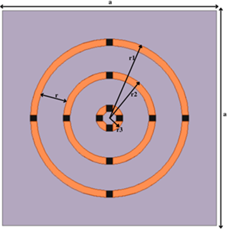
Figure 3. The front view of the proposed unit cell structure.
Numerical simulations and analysis
The design of the proposed unit cell structure of MA was simulated in the commercially available Finite Element Method solver, ANSYS HFSS. To achieve the desired bandwidth of the proposed MA, the optimized dimensions of the unit cell structure are as follows: a = 31.5 mm, r1 = 12 mm, r2 = 7 mm, r3 = 2 mm, r = 4 mm, res1 = res2 = 220 ohm, and res3 = 150 ohm, where res1, res2, and res3 are the resistances of four resistors placed in the outer circle, middle circle, and the inner circle, respectively. Materials found in nature comprise micro-atoms that have magnetization and polarization attributes to determine their electromagnetic (EM) response. However, in metamaterials, EM wave traverse through the electric field and magnetic field, which helps in actuating the electrons present in the atoms. These transmission properties help to modify the consuming energy of incident waves. Permittivity, ε = ε′ + iε″, and permeability, μ = μ′ + iμ″, indicate the degree of motion. The real components of ε and μ specify the polarization and magnetization degree, respectively. However, the imaginary components of ε and μ specify the basic characterization parameters that help in determining the losses in a medium. We have computed wideband absorptivity, A(ω), using equations (1) and (2).
 \begin{equation}A\left( \omega \right) = 1 - {\left| {{S_{11}}\left( \omega \right)} \right|^2} - {\left| {{S_{21}}\left( \omega \right)} \right|^2}\end{equation}
 \begin{equation}A\left( \omega \right) = 1 - {\left| {{S_{11}}\left( \omega \right)} \right|^2}\end{equation}
The computed value of A(ω) depends upon reflected (S 11) and transmitted (S 21) power. As the bottommost layer of the unit cell structure is completely covered with a resonating material, copper, there is no transmission of waves; hence, the transmitted power in equation (1) is zero and the absorptivity becomes completely dependent on reflected power as shown in equation (2). The absorptivity of the unit cell structure can be controlled by manipulating the reflected power from the surface, i.e., lower the value of reflected power, the higher will be the transmitted power and vice versa.
The proposed unit cell structure shows wide bandwidth of 7.62 GHz (2.8–10.42 GHz) along with 99.99% (∼100%) absorption at two distinct peaks, 3.41 GHz and 9.75 GHz, as depicted in Fig. 4.

Figure 4. The simulated absorption of the proposed MA structure.
Theory of absorption
The MA is considered to be a homogeneous medium in order to define the absorption properties. The normalized impedance is evaluated using equation (3).
 \begin{equation}Z = \sqrt {{{{{\left( {1 + {S_{11}}} \right)}^2} - S_{21}^2} \over {{{\left( {1 - {S_{11}}} \right)}^2} - S_{21}^2}}} \end{equation}
As the bottom layer is completely covered with copper and the transmitted power becomes zero, the normalized impedance does not give efficient solution. Hence, the transmitted power plays an important role while computing the normalized impedance.
In order to compute the transmitted power, four small portions of dimension 0.5 × 0.5 mm2 from the bottommost layer are cut from four corners each in such a manner that the absorption frequency does not get altered. Figure 5 depicts the normalized impedance, in which it is observed that in the range of interest (2.8–10.42 GHz), the real and imaginary components approached toward unity and zero, respectively, which clearly indicates the achievement of perfect impedance resulting into maximum absorption.

Figure 5. The normalized impedance.
The real component that approaches toward unity as shown in Fig. 5 occurs due to rapid change in variables of permittivity (ε eff) and permeability (μ eff) at the absorption frequency, eventually satisfying the electric and magnetic resonance conditions, respectively. This is demonstrated in Figs. 6 and 7.

Figure 6. The simulated real components of permittivity and permeability.

Figure 7. The simulated imaginary components of permittivity and permeability.
The effective ε eff and μ eff are computed using electric susceptibility (E s) and magnetic susceptibility (M s) as seen in equations (4–7).
 \begin{equation}{E_{\textrm{s}}} = {{2j{S_{11}} - 1} \over {k{S_{11}} + 1}},\end{equation}
 \begin{equation}{E_{\textrm{s}}} = {{2j{S_{11}} + 1} \over {k{S_{11}} - 1}},\end{equation}
 \begin{equation}{\varepsilon _{{\textrm{eff}}}} = 1 + {{{E_{\textrm{s}}}} \over d},\end{equation}
 \begin{equation}{\mu _{{\textrm{eff}}}} = 1 + {{{M_{\textrm{s}}}} \over d}.\end{equation}
In the above formulae, k demonstrates the wave number and d is the distance traveled by the incident EM wave. The value of refractive index (η) is computed using equation (8) and is shown in Fig. 8.
 \begin{equation}\eta = {1 \over {kd}}{\cos ^{ - 1}}\left[ {{1 \over {2{S_{21}}}}\left( {1 - S_{21}^2 - S_{11}^2} \right)} \right].\end{equation}
Figure 8. Refractive index.
To explain the mechanism of absorption, field distributions are computed at 3.66 GHz and 9.54 GHz. It is observed that the current distributions of the top and bottom surfaces are anti-parallel with reference to each other, as depicted in Fig. 9. As a consequence of the circulating current, magnetic excitation is generated perpendicular to the magnetic field. Also, electric field is induced through electric excitation, as depicted in Fig. 10. As a result, strong EM resonance transpires that maximizes the absorption.

Figure 9. The electric field distribution of the proposed MA. (a) Top surface at 3.66 GHz, (b) top surface at 9.54 GHz, (c) bottom surface at 3.66 GHz, and (d) bottom surface at 9.54 GHz.

Figure 10. The current distribution of the proposed MA. (a) Top surface at 3.66 GHz, (b) top surface at 9.54 GHz, (c) bottom surface at 3.66 GHz, and (d) bottom surface at 9.54 GHz.
It is observed from Figs. 6 and 7 that ε eff and μ eff show a huge deviation near two absorptivity peaks. This proves that the magnetic excitation and the electric excitation occur simultaneously.
Analysis of metamaterial under normal and oblique incidence
To understand the sensitivity of polarization, the proposed MA is examined under normal incident of wave for transverse electric (TE) mode and transverse magnetic (TM) mode, which is further examined under oblique incident for TE and TM mode. For analyzing the absorption, the direction of electric field is kept constant, and the wave vector and direction of magnetic field are varied.
Under normal incident of wave, the reflection coefficient of the proposed MA is measured by rotating the MA from horizontal degree of polarization (ϕ = 0°) to vertical degree of polarization (ϕ = 90°) at every 15° increments. It is spotted that with every increasing angle of polarization, the absorptivity remains the same as depicted in Fig. 11. Hence, it can be said that the proposed MA is polarization insensitive.

Figure 11. The simulated absorptivity curve under normal incidence.
The proposed MA is further inspected under oblique incident of wave to study the polarization properties for TE and TM mode, where the reflection coefficient of the structure is measured by rotating the MA from horizontal degree of polarization (ϕ = 0°) to vertical degree of polarization (ϕ = 90°) at every 15° increments. It is spotted from Figs. 12 and 13 that the absorptivity decreases with an increase in the angle of incidence.

Figure 12. The simulated absorptivity curve under oblique incidence for TE polarization.

Figure 13. The simulated absorptivity curve under oblique incidence for TM polarization.
Measurement setup
The MA presented in this article was fabricated on a Duroid sheet of 31.5 cm × 31.5 cm containing 10 × 10 unit cells. A copper sheet is used to cover the bottommost layer of the proposed MA. The entire setup is placed inside the anechoic chamber. The VNA is used to calculate the absorption of the proposed MA under normal incidence. This experimental setup consists of two horn antennas, among which one acts as a transmitting antenna and the other acts as a receiving antenna, as depicted in Fig. 14. Figure 15 portrays the simulated and the measured results of the proposed MA; it is perceived from the graph that the results are in compliance with each other.

Figure 14. The experimental setup inside anechoic chamber. (a) Metamaterial absorber, (b) transmitting horn antenna, (c) receiving horn antenna, and (d) vector network analyzer.

Figure 15. The absorption plot for simulated and measured results.
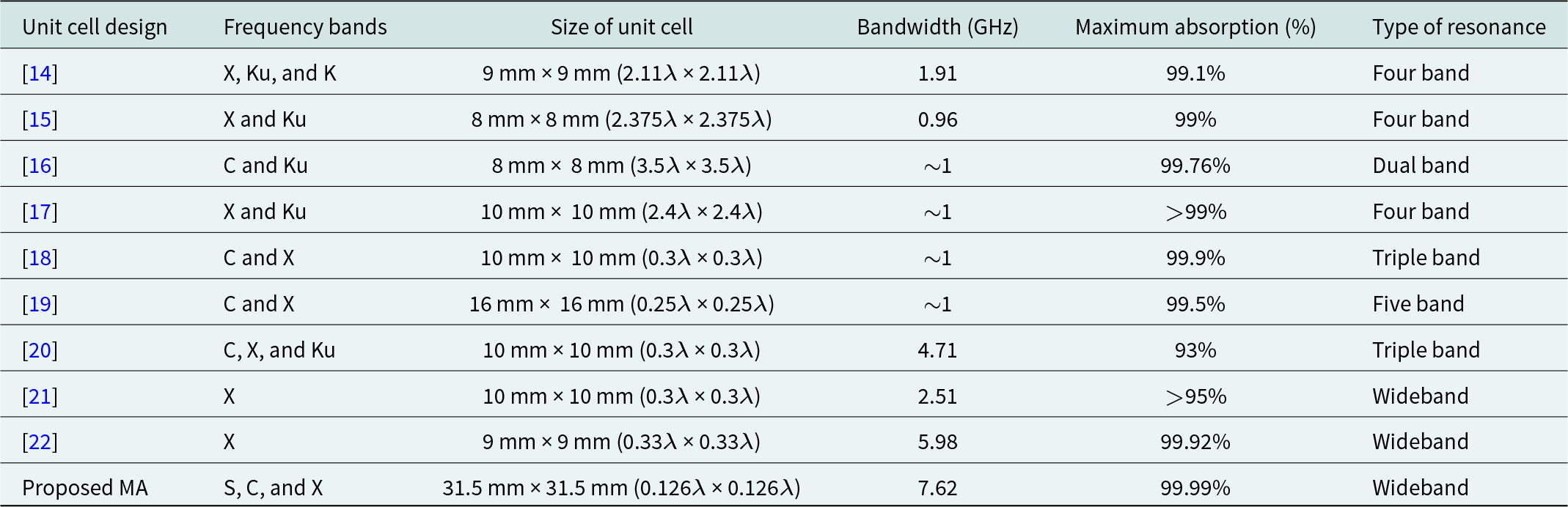
Table 1 shows the comparison between our proposed MA and the MAs investigated in the literature. The comparison concerns with the resonance frequencies, bandwidth, and the absorption of the unit cell structures. It is observed that the proposed MA achieves a better bandwidth as compared to the other MAs.
Table 1. Comparison between the proposed work and MAs investigated in literature
The tested and simulation plots are measured and shown in Fig. 16. From the plot, it is observed that the tested and simulated results are close in the agreement.

Figure 16. Arrangement inside anechoic chamber.
Conclusion
The MMA stated in this report is angle independent. The structure is built on an FR4 substrate having single cell dimension of 31.5 mm × 31.5 mm × 10.805 mm. The layout includes two concentric circle that are linked by consolidated resistors. The absorptivity is achieved above 90% in the range from 2.8 and 10.42 GHz, which conclude wide band of 7.62 GHz. Within this range, two peaks, i.e., 3.66 and 9.54 GHz, are considered for the analysis purpose. Parametric considerations are made in terms of substrate height, height of air aperture, and resistor. The refined results acquired post the performing parametric observations are represented as absorptivity versus frequency plots. To confirm the metamaterial properties acquired by the presented structure, permittivity (ε) and the permeability (μ) are considered. Wide band absorption phenomenon is proven with the help of current and electric field distribution. The presented structure is angle independent for phi variation. The fabricated sheet that consists of array of unit cell are examined inside the anechoic chamber with the help of two horn antennas and VNA. The result obtained from the chamber is compared with the simulated one, and it is observed that they both are close in their agreements. At last, the presented and already reported state of arts are compared and found that the presented one is used for low frequency with wide bandwidth. The presented MMA find practical applications in the field of defense for RCS reduction.

Rajyalakshmi G received her B.E. degree in Electronics & Communications Engineering from Chaitanya Bharati Institute of Technology, Hyderabad, in 2000 and her M.E. in Electronics & Communication Engineering from Osmania University, Hyderabad, in 2002. Presently, she is pursuing PhD from Osmania University, Hyderabad. She was a Scientist/Engineer at Aeronautical Development Agency (ADA), Bangalore, from 2004 to 2010. She joined Bharat Dynamics Limited (BDL), Hyderabad, in 2010 and is presently working as a Senior Manager in RF Seekers production division. Her area of specialization is Microwave Antennas and Radar Engineering for military applications. Her current interest is in microwave antennas based on metamaterials. She has published papers in international conferences/Journal proceedings. She is a student member of IEEE and a Life member of ISTE.

Y Ravikumar was born in Machilipatnam, Andhra Pradesh, on November 3, 1959. He obtained his B.Tech. ECE (Electronics and Communication Engineering) from the College of Engineering, Kakinada, in 1981 and M.E. (Microwave & Radar Engineering) from Osmania University in 1984 and PhD from Osmania University in 2007. He has put up 36 years of service in DLRL. Presently, he is heading HMD under the directorate of Antennas. He had 36 years of research experience in antennas, communications, and system integration.

Dr. D. Rama Krishna received his Bachelor of Technology (B.Tech.) in Electronics and Communications Engineering from Sri Krishna Devaraya University, Ananthapur, Andhra Pradesh, India, and obtained his Master of Engineering (M.E.) and Doctor of Philosophy (Ph.D.) in Electronics and Communication Engineering from Osmania University, Hyderabad, Telangana, India. He joined as an Assistant Professor in the Department of ECE, University College of Engineering, Osmania University, in the year 2007; presently, he is working as Professor and Chairperson Board of Studies (University) for the Department of ECE, Osmania University, and also Serving as Director for Centre for Excellence in Microwave Engineering (CEME), University College of Engineering, Osmania University.

Sambasiva Rao Kumbha received his B.Tech. Degree in Electronics and Communication Engineering in 2003 from NIT, Warangal, India. He received M.E. degree in Microwave and Radar Engineering from Osmania University, Hyderabad, India. Presently, he is pursuing Ph.D. from IIT Tirupathi. He was a Technical officer in ECIL, Hyderabad, from May 2005 to June 2009. He joined Research Center Imarat, DRDO, Hyderabad, in June 2009 and presently working as Scientist-E in Radar Antennas and Components Division. He is a Senior Member of IEEE, Antennas and Propagation Society and Microwave Theory and Techniques Society.


