


Introduction
Planar reconfigurable antennas have fascinated a lot of attention in the fastest development of microwave radio frequency wireless transmission services. The features such as small size, lightweight, cost-effective, and ease of integration with other communication systems make them an ideal component of today’s modern communication system [Reference Reji and Manimegalai1]. The reconfigurable antenna brilliantly diversifies its resonance frequency, radiation pattern, and polarization by tuning/switching mechanism [Reference Mamta and Mittal2]. There are numerous techniques for reconfigurability using switches (electrical, optical, and mechanical), actuators (motors and linear actuators), and material change (plasmonic and liquid crystal) [Reference Ojaroudi Parchin, Jahanbakhsh Basherlou, Al-Yasir, M. Abdulkhaleq and A. Abd-Alhameed3]. Electrical switching methods including PIN diode, varactor diode, field effect transistor, and radio frequency-MEMS (Micro Electro Mechanical Systems) are the most famous among all the methods due to their fast switching, ease of integration with the other system, and high rate of repeatability [Reference Jenath and Nagarajan4–Reference Aboufoul, Alomainy and Parini7]. The reconfigurable antenna has the capability to accommodate various new microwave services depending on public demand and utility and simultaneously support multiple wireless spectrums according to FCC (Federal Communications Commission) standards.
Some of the reconfigurable antennas have been studied for the literature survey. In papers [Reference Mamta, Kumar, Mittal and Suman8, Reference Borhani Kakhki and Rezaei9], a frequency-diversified antenna has been demonstrated that is capable to switch/tune its resonating frequency by changing the biasing state of the electronic switches such as PIN/varactor diode. They can absolutely eliminate the sophisticated bandpass filters used in almost all wide-band antennas. A pattern reconfigurable antenna proposed in paper [Reference Zhang, Songnan Yang, Fathy, El-Ghazaly and Nair10] scans the main beam from −70° to +70° in the H-plane by changing the capacitance of the varactor diode incorporated in the main patch. A simple polarization reconfigurable antenna with a two-probe feed network [Reference Yang and Luk11] was analyzed for RHCP and LHCP (left-hand and right-hand circular polarization) by connecting the main patch with the probe feed network using two PIN diodes. Frequency diversified antenna provides frequency switching over the desired frequency range, and it efficiently utilizes the frequency spectrum [Reference Hinsz and Braaten12, Reference Akyildiz, Lee, Vuran and Mohanty13]. Radiation pattern reconfigurable antenna provides the beam directed towards the intended direction with high gain and thus saves energy [Reference Dong, Li and Zhang14], and it also suppresses out-turn of in-band interference resulting in improved channel capacity. Polarization antennas have the capability of configuring themselves for different modes of polarization [Reference Borhani, Rezaei and Valizade15, Reference Lee and Sung16]. They can switch between horizontal polarization, vertical polarization, and circular polarization (LHCP and RHCP) and can be used to reduce polarization mismatch losses in portable devices.
Recently, many novel concepts and fascinating strategies have been described for achieving reconfigurability in antenna with defected ground structure (DGS) implementation. The ground plane having some slot in it is referred as DGS that results in size miniaturization, mutual coupling reduction, and suppressed surface wave [Reference Fakharian, Rezaei and Orouji17]. Here, some of the magnificent concepts of DGS-based reconfigurable antennas are summarized in papers [Reference Shah, Hayat, Khan, Ullah and Afridi18–Reference Madhav, Rajiya, Nadh and Kumar22].
In paper [Reference Shah, Hayat, Khan, Ullah and Afridi18], a frequency-diversified 9-shaped monopole antenna in which the ground surface is truncated has been investigated for multiple wireless applications such as Wi-Fi, WLAN, and Wi-MAX. Further, an unequal E-shaped DGS-based semi-transparent (glass substrate) frequency reconfigurable antenna is proposed in paper [Reference Lim, Rahim, Hamid, Soh and Eteng19], investigating four different operating frequencies between 3 and 6 GHz. In paper [Reference Sathikbasha and Nagarajan20], a modified ground-based frequency reconfigurable antenna is introduced by embedding a U-shaped and an I-shaped slot in the ground to achieve multiple bands. A frequency reconfigurable antenna is designed in paper [Reference Han, Wang, Chen and Zhang21], which is desirable for wireless communication applications. It has a rectangular U-shaped slot and L-shaped slot antenna that is able to resonate at three frequencies 2.3 GHz, 4.5 GHz, and 5.8 GHz. After going through the various published articles, it has been observed that antenna size needs to be further miniaturized without compromising gain.
This paper presents a circular microstrip G-slotted patch DGS-based antenna for reconfigurable/switchable operating frequencies. The prototype antenna is suitable for operating in four different operating states. This innovative antenna structure exhibits higher gain with compact size. To design this antenna, three PIN diodes are incorporated out of which two PINs are integrated within DGS and one PIN is used between the slot in the patch. Lots of modifications in the ground and patch with proper diode position have been done and simulated on software to find the best performance of the antenna. Performance characteristics of the designed antenna such as its reflection coefficient, gain, and radiation pattern are discussed with the comparison of simulated and measured results in the further section of this paper. In the next section, the antenna geometry is discussed. The upcoming section discusses the proposed work and its flow sequence. The subsequent section discusses the results and analysis. At last, the conclusion is drawn with the extension in the near future.
Antenna design configuration and its methodology
The shape of the proposed reconfigurable antenna along with all its defined design parameters is depicted in Fig. 1. The antenna is printed on both sides of the Roger RT/Duroid 5880 substrate having a relative permittivity of 2.2, a relative permeability of 1, and a dielectric loss tangent of 0.0009. Roger substrate is little bit more expensive as compared to fiber glass, but it has less dielectric loss tangent making it preferable for high-frequency RF (Radio Frequenc) circuits. The final structure of the antenna is a modified form of the basic circular-shaped radiator. The geometry of the proposed antenna has dimensions of 30 mm × 27 mm × 1.6 mm. A Sub-Miniature version A (SMA) connector is connected to the feed line of width 2.25 mm resulting in a characteristic impedance of 50 Ω for proper transmission of a signal to the radiator. From Fig. 1, it is very clear that the patch consists of one PIN diode and ground has two PIN diodes. The proposed antenna provides switching between four different frequency bands.
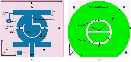
Figure 1. Geometry of the proposed designed antenna: (a) front view and (b) back view.
The dimension of all parameters used to design the final proposed circular antenna is listed in Table 1.
Table 1. Dimensions of antenna parameter
Evaluation of the antenna structure from basic circular antenna structure to the final proposed antenna structure is performed in four stages as shown in Fig. 2. Figure 4 each structure mentioned in Fig. 2 of different stages is simulated and observed its return loss value plotted in Fig. 3. The antenna design methodology is explained in Fig. 4 in the form of a flow chart in which all steps are mentioned to achieve the final antenna design.

Figure 2. Evaluation stages of proposed antenna.
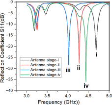
Figure 3. Reflection coefficient of four evaluation stages of proposed antenna.

Figure 4. Flowchart of antenna design methodology.
The reflection coefficient of the proposed antenna at different evaluation stages is plotted in Fig. 3. The return loss plot helps in finalizing the final stage of the antenna. It is clear from the plot that the return loss (S11) improved from structure (i) to (iv) from −22 dB to −37 dB, and stage (iv) became the final proposed antenna. The above return loss plot of the antenna shown in Fig. 3 is before inserting PIN diodes in the structure.
These are the antenna design equations used to find the dimension of the circular patch mentioned in [Reference Mamta, Mittal and Raheja6].
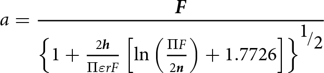 \begin{equation}{{a}} = \frac{{\boldsymbol{F}}}{{{{\left\{ {1 + \frac{{2{\boldsymbol{h}}}}{{{{{\Pi \varepsilon rF}}}}}\left[ {\ln \left( {\frac{{{{{\Pi F}}}}}{{2{\boldsymbol{n}}}}} \right) + 1.7726} \right]} \right\}}^{{\raise0.7ex\hbox{$1$} \!\mathord{\left/
{\vphantom {1 2}}\right.}
\!\lower0.7ex\hbox{$2$}}}}}}\end{equation}
\begin{equation}{{a}} = \frac{{\boldsymbol{F}}}{{{{\left\{ {1 + \frac{{2{\boldsymbol{h}}}}{{{{{\Pi \varepsilon rF}}}}}\left[ {\ln \left( {\frac{{{{{\Pi F}}}}}{{2{\boldsymbol{n}}}}} \right) + 1.7726} \right]} \right\}}^{{\raise0.7ex\hbox{$1$} \!\mathord{\left/
{\vphantom {1 2}}\right.}
\!\lower0.7ex\hbox{$2$}}}}}}\end{equation}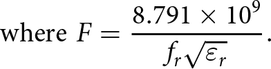 \begin{equation}{\textrm{where}}\,\,F = {{8.791 \times {{10}^9}} \over {{f_r}\sqrt {{\varepsilon _r}} }}.\end{equation}
 Equation (1) provides the radius of the circular patch without considering the fringing effect of the patch. Fringing makes the size of the patch electrically larger than the original one. So, the effective radius ( ${a_e}$) of the patch is considered for calculating the more accurate value of resonant frequency mentioned in equation (3)
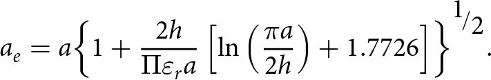 \begin{equation}{a_e} = a{\left\{ {1 + {{2h} \over {\Pi {\varepsilon _r}a}}\left[ {\ln \left( {{{\pi a} \over {2h}}} \right) + 1.7726} \right]} \right\}^{{\raise0.7ex\hbox{$1$} \!\mathord{\left/
{\vphantom {1 2}}\right.}
\!\lower0.7ex\hbox{$2$}}}}.\end{equation}
\begin{equation}{a_e} = a{\left\{ {1 + {{2h} \over {\Pi {\varepsilon _r}a}}\left[ {\ln \left( {{{\pi a} \over {2h}}} \right) + 1.7726} \right]} \right\}^{{\raise0.7ex\hbox{$1$} \!\mathord{\left/
{\vphantom {1 2}}\right.}
\!\lower0.7ex\hbox{$2$}}}}.\end{equation} Hence, the resonant frequency for the patch having effective radius  ${a_e}$ with dominant TMZ110 is represented by equation (4) mentioned in [Reference Mamta, Mittal and Raheja6]:
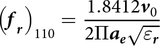 \begin{equation}{\left( {{{\boldsymbol{f}}_{\boldsymbol{r}}}} \right)_{110}} = \frac{{1.8412{{\boldsymbol{v}}_0}}}{{2{{{\Pi }}}{{\boldsymbol{a}}_{\boldsymbol{e}}}\sqrt {{{{{\varepsilon }}}_{\boldsymbol{r}}}} }}\end{equation}
 In the above equations  ${\varepsilon _{r\,}}$ is denoted as dielectric constant,
  ${v_0}$ is denoted as the speed of light and h is the thickness of the substrate. After designing the proposed antenna for 5 GHz based on the above equation, G-slot on the patch and circular slot on the DGS is introduced to increase the electrical length. Switching electronic element PIN diode with notably low junction capacitance is preferred as RF switch between the slot in the patch and ground. PIN diode, BAP-65 is pick out for this frequency diversified antenna, due to its highly acceptable electrical parameters depicted in Table 2.
Table 2. PIN diode equivalent circuit parameter
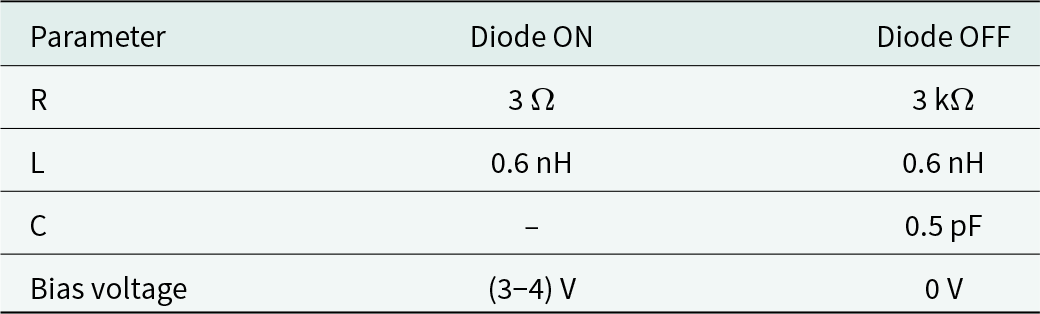
PIN diode equivalent circuit and its biasing circuit are shown in Fig. 5(a) and (b). PIN diode works in either OFF/ON mode for 0–4 V, respectively, and it is controlled by using an external battery. The electrical equivalent circuit of the PIN diode switch in forward bias (ON state at 3–4 V) is equivalent to 3 Ω resistor and inductance of 0.6 nH, whereas PIN in reverse bias (OFF state at 0 V) conditions, it offers high resistance of 3 kΩ with capacitance of 0.5 pF and inductance of 0.6 nH as shown in Table 2. Model of PIN diode using RLC boundary is simulated in ANSYS Electronics Desktop 2018.2 software to add and analyze the effect of PIN diode in actual antenna design. Simulation result of the transmission loss/insertion loss and S21 of PIN diode for forward bias and reverse bias condition are plotted in Fig. 6. Simulated results shows that PIN diode in ON condition provides transmission loss of average −0.6 dB from 2 to 5 GHz; hence, it is clear that PIN in forward bias condition will offer low impedance and act as short circuit for RF signal. On the other hand, when PIN diode in OFF condition provides insertion loss below −17 dB, it offers very high impedance, and hence there is no propagation of RF signal power from source to load terminal.
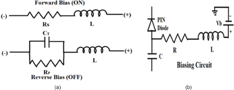
Figure 5. (a) Equivalent electrical circuit for PIN diode in forward bias and reverse bias and (b) biasing circuit for PIN diode.
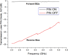
Figure 6. Transmission loss of PIN diode in forward bias and reverse bias.
In order to provide DC bias for switching the PIN diode and to simultaneously decouple the RF signal from the DC bias, two biasing cum decoupling elements are also designed with the main radiating patch as shown in Fig. 1(a), and equivalent biasing circuit for PIN diode is represented in Fig. 5(b). The thin line of the biasing circuit acts as an inductor and the small rectangle acts as a capacitor, and the combination of both acts as a low pass filter.
As per the dimension for a proposed antenna in Table 1 and PIN diode configuration in Table 2, the antenna is designed and simulated. The designed antenna reconfigures its operating frequency to four different bands controlled by the biasing of the PIN diode. All the results are discussed in the further section.
Results and discussion
Parametric analysis for finalizing the antenna design
In the process of designing the final proposed antenna, the G-slot is introduced in the main radiating patch as shown in Fig. 1(a). The parametric analysis has been done to optimize the antenna performance and fix the g-length associated with G-slot. A parametric study is performed and a return loss plot is obtained for different values of “g” in mm (3.5, 4.0, 4.5, 5.0, and 5.5) as shown in Fig. 7. It gives the best S11 at 4.5 mm with 27 dB and so “g” is fixed at 4.5 mm.

Figure 7. Return loss plot for parametric study for “g”-length.
Return loss (S11) vs frequency
Figure 8 presents the top and bottom view of the fabricated antenna on Roger substrate of height 1.6 mm as per the dimension in Table 1 for “g” 4.5 mm. Before the testing, one BAP-65 PIN diode is mounted at the proper place on the radiating patch shown in Fig. 8(a), and two diodes are mounted between the outer circle and inner circle shown in Fig. 8(b). The outer circle and inner circle are connected or disconnected depending on the biasing condition of PIN 2 and PIN 3. Current distribution and change in electrical length cause the change in resonance frequency for the different biasing conditions of the diodes connected at the patch and ground.
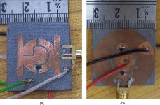
Figure 8. Picture of the fabricated reconfigurable antenna: (a) top view and (b) bottom view.
The antenna is tested for return loss (S11) using Anritsu Vector Network Analyzer (VNA) (MS2038C). The VNA is calibrated by Short-Open-Load-Through method before testing the antenna. Figure 9 shows the pictures taken at the time of S11 measurement through the VNA for two different cases.
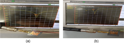
Figure 9. (a) S11 on VNA for case 1 and (b) S11 on VNA for case 2.
Simulated and measured reflection coefficient plot (S11) is plotted and compared in Fig. 10 for all four different cases. It is observed from the plot that the measured results are very near to the simulated results and both plots are well matched. The measured return loss has a little bit of frequency offset with the simulated one because of the integration of lumped switches (PIN-diode) on the fabricated antenna, cable loss, connector (SMA) loss, and fabrication tolerance.
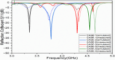
Figure 10. Return loss for case 1 (PIN 1 – ON, PIN 2 – OFF, PIN 3 – ON), case 2 (PIN 1 – ON, PIN 2 – OFF, PIN 3 – OFF), case 3 (PIN 1 – OFF, PIN 2 – ON, PIN 3 – OFF), and case 4 (PIN 1 – OFF, PIN 2 – ON, PIN 3 – OFF).
Due to the PIN diode in the structure, it acts as a resistive load in the ON state and causes conductive loss in the antenna. Since the PIN diode is integrated into the antenna substrate, it introduces dielectric losses due to the material’s inherent properties. The switching loss of the PIN diode between their ON/OFF states incurs losses leading to a decrease in the overall efficiency. In the ON state, the PIN diode acts as an additional component in the signal path causing insertion losses that reduce the effective radiation power. So, there is a little bit of frequency offset between the tested and simulated result shown in Fig. 10. From the S11 plot, it is very clear that the proposed antenna is resonating at 3.35 GHz, 3.78 GHz, 4.32 GHz, and 4.55 GHz for case 1, case 2, case 3, and case 4, respectively.
Case 1 is the case when PIN 1 ON, PIN 2 OFF, and PIN 3 ON provides an antenna for WiMAX application at the resonating frequency of 3.35 GHz with S11 −30 dB and gain 3.3 dBi. Case 2 is the case when PIN 1 ON, PIN 2 OFF, and PIN 3 OFF provides an antenna suitable for satellite communication at an operating frequency of 3.78 GHz with S11 −35 dB and gain 3.7 dBi. When PIN 1 OFF, PIN 2 ON, and PIN 3 OFF refers to case 3 which makes the antenna suitable for aeronautics at a resonating frequency of 4.32 GHz with S11 −30 dB and gain 3.8 dBi. When PIN 1 OFF, PIN 2 OFF, and PIN 3 ON is the fourth case that provides an antenna applicable for mobile communication at the operating frequency of 4.55 GHz with S11 −28 dB and gain 4.0 dBi.
Further, the behavior of antenna is analyzed from Fig. 11 for case 1 in the form of surface current distribution on the top and bottom of the antenna. For different cases, the path of current changes according to the PIN bias condition, and it results in a change in the effective electrical length of the antenna and hence a change in its operating frequency. The proposed antenna is able to reconfigure its operating frequency for four frequency bands depending on the switching condition of three PIN diodes.

Figure 11. Surface current distribution of (a) top and (b) bottom of the antenna.
Gain and radiation pattern
The fabricated prototype is tested for radiation pattern in the Anechoic chamber. In the Anechoic chamber, 6 dB log periodic reference antenna is placed at a distance of 3 m from the antenna to be tested placed on the turn table for far-field measurement. The turn table rotates the antenna 360° with 10° steps in E-plane and H-plane both. The whole system is controlled from outside the chamber. Figure 12(a) and (b) are the pictures of the Anechoic chamber at the time of taking reading for plotting gain and radiation pattern.
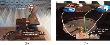
Figure 12. Inside the Anechoic chamber: (a) mechanical rotation system and (b) antenna under test.
Gain of the antenna is presented in 3D form as shown in Fig. 13. It is very clear from the figure that the gain of the antenna varied in the range from 3.3 dBi to 4.0 dBi for different operating frequencies. The achieved gain is justifiable for the application mentioned before.
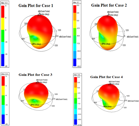
Figure 13. 3D gain plot for case 1 to case 4.
The measured and simulated normalized E-plane (yz-plane) and H-plane (xz-plane) patterns are plotted and compared in Fig. 14 for all four cases. From the figure, it is very clear that the H-plane pattern of the antenna is distorted omnidirectional and E-plane pattern is adopting a shape like ‘8’ along with a null lobe at 270° and 90°. The introduction of DGS can potentially alter the EM (Electromagnetic) coupling between the patch and ground plane, affecting the antenna resonant frequency and radiation characteristic. Proper design and placement of DGS can lead to unintended changes in the radiation pattern degrading the antenna’s performance. From Fig. 14, it is observed that back lobe levels are high, which may be due to DGS and the asymmetrical shape of the antenna design. In this shape, the surface wave on the substrate can couple with the patch, which causes increased radiation in undesired directions, such as back lobes. The terminated edge of the patch is just above the ground plane, and it can also cause diffraction leading to back lobe radiation. It is analyzed from the radiation pattern that as operating frequency increases from case 1 to case 4, the directivity increases or in other words half power beamwidth goes on decreasing.

Figure 14. Radiation pattern for all cases.
Comparison study
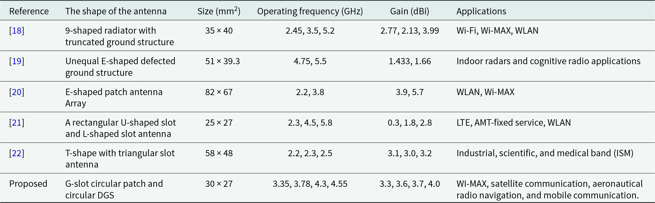
In Table 3, comparative study has been provided with respect to antenna model, size, gain, and its application keeping the size minimal. It is observed that the proposed antenna is smaller in size compared to all the similar antennas reported in Table 3 except reference [Reference Han, Wang, Chen and Zhang21]. Although it is clear from the table that the proposed antenna is better in aspect that it exhibits appreciable amount of gain than the antenna described in reference [Reference Han, Wang, Chen and Zhang21].
Table 3. A detailed comparison has been mentioned for a similar type of antenna model
Conclusion
In this paper, a compact G-slot circular reconfigurable microstrip antenna with a circular DGS structure is analyzed. It has the capability of changing its operating frequency for four different microwave wireless applications. Reconfigurability of the proposed antenna is become possible by introducing three PIN switching diodes, among which one is shouldered in the patch and two PIN in the ground at appropriate places in the slot to achieve four different wireless applications. It may be used for aeronautical radio navigation at 4.3 GHz with a gain of 3.6 dBi, satellite communication at 3.78 GHz with a gain of 3.7 dBi, mobile communication at 4.55 GHz with a gain of 4.0 dBi, and WIMAX at 3.35 GHz with a gain of 3.3 dBi. A simulated and measured result of the fabricated antenna has been performed to demonstrate its desirable characteristics and features.
Acknowledgements
The research work has been well supported by the USICT Department of GGSIP University, Dwarka, New Delhi, India as well as the Advanced Microwave & Antenna Testing Laboratory of the G.B. Pant DSEU Okhla I Campus, New Delhi, India.
Competing interests
The authors declare that they have no known competing financial interests or personal relationships that could have appeared to influence the work reported in this article.

Mamta is currently pursuing her Ph.D. degree from USICT, GGSIP University, Delhi, India. She has done her B.Tech in Electronics and Communication Engineering from Dr. A. P. J. Abdul Kalam Technical University (formerly UPTU), Lucknow, India in 2006 and M. Tech. in Digital Communication Engineering from GGSIP University, Delhi, India, in 20012. She has a teaching experience of more than 12 years including UG and PG courses. She has published more than 10 papers in the national and international conferences and journals. Her research areas include electromagnetic field theory, antenna theory, optical fiber communication, etc.

Vandana Nath has received Ph.D. degree from the University of Delhi in 2005, New Delhi, India. She is Professor (ECE) with USIC&T, Guru Gobind Singh Indraprastha University, New Delhi, M.Sc. (Electronics) from GGDU, Bilaspur and M.Tech (ECE) from GGSIP University. She has more than 23 years of teaching and research experience. She has authored or co-authored more than 50 research papers in international journals and conferences of repute. Her current research area includes analytical modeling, design, and simulation of non-classical MOSFET and HEMT devices and antenna design. She is a member of IEEE and life member of Indian Society of Technical Education (ISTE) and Semiconductor Society of India (SSI).


