Introduction
Wide Band Gap (WBG) semiconductors are important for the development of high-temperature and high-power electronics. For these applications, SiC, GaN, and their heterostructures have been identified as potential candidates due to their wide band gaps, desirable electronic and optical properties, thermal and chemical stability, doping capabilities and the possibility of their use in fabricating high quality heterostructures and devices [Reference Nakamura and Fasol1-Reference Strite and Morkoc2]. The most significant challenge in this area is the fabrication of high quality metal-oxide-semiconductor structures. High quality thin dielectric films having low leakage currents at temperatures up to 450°C under operating fields of about 1 MV/cm are necessary for the high temperature electronics. Thin films of AlN seem to be promising for these applications compared to other materials such as SiO2 An additional advantage of using AlN on SiC or GaN is the very small lattice mismatch (∼5%). Although AlN has been investigated previously [Reference Zetterling, Wongchotigul, Spencer, Harris, Wong and Ostling3-Reference Ouisse, Schenk, Karmann, Kaiser, Pensl, Morkoc, Monemar and Janzen5], its full potential as a dielectric material has not been successfully demonstrated due to many problems associated with the defects such as columnar structures, threading dislocations, and low angle grain boundaries. These defects are responsible for leakage currents at room temperature as well as at elevated temperatures.
In general, the lattice and structural mismatches and the film-substrate interfaces are the dominating parameters governing the microstructure of the AlN films and hence their properties. Conventional growth techniques such as chemical vapor deposition (CVD) and molecular beam epitaxy (MBE) are based on the equilibrium growth conditions and produce columnar structures in the III-V nitrides on SiC and sapphire. A highly non-equilibrium growth process is desirable to circumvent these growth problems. For example, energetic processes involved in the non-equilibrium growth conditions can be utilized to form stacking faults in the plane of the interface to manage the lattice mismatch induced strain rather than the formation of vertical threading dislocations, or columnar structures in the films. Such energetic and non-equilibrium growth conditions can be achieved, for example, in Pulsed Laser Deposition (PLD) [Reference Vispute, Choopun, Enck, Patel, Talyansky, Sharma, Venkatesan, Sarney, Salamanca-Riba, Andronescu, Iliadis and Jones6]. Such a process can be utilized in the early stages of growth of the dielectric layer without the formation of columnar structures or vertical grain boundaries. In this paper, we highlight the growth of AlN films by PLD, their characterization, and their application for the development of high-temperature SiC based thyristors. Our major objective is to develop and fabricate thyristors based on SiC, with integration of other wide band gap materials suitable for high-temperature operation (300-500 °C). In this context, we have studied the suitability of the PLD technique for the fabrication of AlN thin films for encapsulation, passivation, and as a dielectric layer on SiC.
Experimental
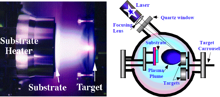
The schematic of the PLD process is shown in Fig. 1. A KrF excimer laser (λ = 248 nm, τ = 25 ns) was used for the ablation of a polycrystalline, stoichiometric AlN target (99.99 purity) at an energy density of ∼1 J/cm2. Upon laser absorption by the target surface, a strong plasma plume is produced as shown in Figure 1. The laser-induced plasma consists of atoms, molecules, excited atomic and molecular species, and clusters. The laser ablated species are allowed to condense on to a substrate kept at suitable temperature. The NH3 background gas pressure in our experiment was varied from 10−6 to 10−3 Torr. The deposition rate and the film thickness were controlled by the pulse repetition rate (5 to 10 Hz) and total deposition time (30 to 60 min.). The PLD films were characterized by four-circle x-ray diffraction (XRD), atomic force microscopy (AFM), UV-visible spectroscopy, Rutherford backscattering spectrometry (RBS) and ion channeling, transmission electron microscopy (TEM), and electrical transport (I-V) measurements. TEM studies were performed using JEOL 2010 system operated at 200KV.

Figure 1. Laser induced plasma plume of III- nitrides and schematic of the PLD.
Results and Discussion
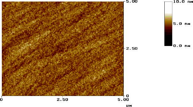
The crucial parameters in the PLD of AlN dielectric films are the deposition temperature and laser fluence. We have studied the dependence of these parameters on the crystalline quality, surface morphology, and the optical and electrical properties of the III-V nitride films [Reference Vispute, Choopun, Enck, Patel, Talyansky, Sharma, Venkatesan, Sarney, Salamanca-Riba, Andronescu, Iliadis and Jones6]. We found that AlN grows epitaxially on sapphire, SiC, and GaN at a substrate temperature as low as 600 °C. However, the crystalline quality of these films improves with an increase in the substrate temperature. High epitaxial quality was obtained when the films were grown under a NH3 background gas pressure of 5×10⁻⁵ Torr and a substrate temperature of 850 to 1000 °C. The XRD θ−2θ angular scans of a 2000-5000 Å thick film clearly show only a {000l} family of the planes of wurtzite-AlN with full-width-at-half-maximum (FWHM) of the rocking curve (ω) for the (0002) peak of about 5 to 7 arc-minutes. The quantitative analysis of the crystalline quality, composition, and interface structure of the III-V nitride films was carried out by RBS and ion-channeling techniques. The ratio of the RBS yield with the He+ beam incident along [0001] (channeled) to that of a random direction, respectively, (χmin), reflects the epitaxial quality of the film. Figures 2 show the aligned and random backscattering spectra for the AlN films. The χmin near the surface region of the films is ∼3%, indicating a high degree of crystallinity. This χmin value is close to that of high quality MOCVD and MBE films. measured by AFM for AlN (Figure 3) was ∼ 0.5 to 2 nm. The mean surface roughness of 0.5 nm obtained for the AlN film grown at 1000°C is essentially the unit cell height of the AlN. The high vacuum conditions have also enabled us to grow pinhole free, uniform films with low lattice stress which are crucial factor for the encapsulation of ion implanted SiC and the fabrication of device quality dielectric layers.

Figure 2. RBS and ion channeling spectra of PLD AlN dielectric film on 6H-SiC (0001).

Figure 3. AFM of PLD AlN thin film deposited on SiC.
Microstructural characteristics, epitaxy, and interfaces were characterized using high-resolution transmission electron microscopy. TEM studies indicated that the PLD AlN films grown above 700 °C were epitaxial and single crystalline. As-grown films on 6H-SiC are essentially single crystalline of good crystallographic quality as revealed by selective area diffraction (SAD) pattern (not shown) and the contrast from the micrographs in imaging mode. Observation in low magnification of the AlN film also showed uniform contrast indicating high crystalline quality of the film. Figure 3 shows high-resolution TEM lattice image of AlN/SiC interface. In the HRTEM investigation, we observed numerous stacking faults than the threading dislocations. This is in contrast to the columnar structures usually observed for the III-V nitrides grown by CVD and MBE. At the present juncture, we feel that the growth process in the pulsed laser deposition of AlN is away from equilibrium conditions due to high kinetic energy and instantaneously high arrival rate of the laser ablated particles. Note also that the interface with the 6H-SiC substrate is clean, smooth, and shows no indication of amorphous phase.
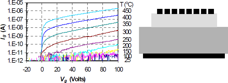
Epitaxial TiN gate electrodes with low resistivity were fabricated using pulsed laser deposition of TiN at 600C [22]. The TiN/AlN/SiC MIS capacitors with gate areas of 4×10⁻⁴ cm2 were patterned using ion milling, and high-temperature current-voltage (I-V) characteristics and were studied up to 450 °C. The thickness of the AlN films used as a dielectrics was varied from 200 nm to 600 nm. A typical substrate for these studies was research grade Si face-6H-SiC, 3.5° off and highly doped (4×1017cm−3) n-type. We measured leakage current densities of around 10−8 A/cm2 at room temperature and of around 7*10−3 A/cm2 at 450 °C for a 1.7 MV/cm field, as shown in Fig. 4. These leakage currents are orders of magnitude lower than values that have ever been previously reported for AlN thin films. The mechanism of the leakage currents in PLD AlN films at high temperature is discussed in our earlier papers [Reference Scozzie, Lelis, McLean, Vispute, Patel, Sharma and Venkatesan7-Reference Scozzie, Lelis, McLean, Vispute, Patel, Sharma and Venkatesan8]. It is now interesting to note that the microstructure of the PLD AlN described earlier is responsible for the low leakage current densities.

Figure 4. HRTEM of PLD AlN dielectric film on 6H-SiC(0001) substrate.

Figure 5. I-V characteristics and schematic of PLD TiN/AlN/SiC MIS capacitors
We have shown that high-quality thin films of AlN can be fabricated by PLD at substrate temperatures (750 to 850 °C) which are lower than those employed in (MOCVD) (1000 to 1100 °C), an alternate growth method. These films show a high degree of crystallinity and good optical properties. Most importantly, the PLD AlN films show leakage current densities below 10E-08 A/cm2 at room temperature and about 5×10⁻³ A/cm2 at 450°C under 2 MV/cm accumulation field. Their properties of PLD AlN are excellent for its applicability as a dielectric for SiC thyristors. The interfaces between the AlN and SiC were sharp. PLD is also used successfully for epitaxial growth of TiN ohmic contacts. It is demonstrated that the PLD AlN films on SiC substrates do not have the usual columnar structure that allows grain boundaries to propagate parallel to the c-axis. Rather, the mismatch strain appears to be mostly accommodated by the formation of stacking faults. Since these defects are parallel to the SiC/AlN interface, it may be possible to fabricate high quality MIS SiC device structures. After the growth of a critical thickness of the dielectric layer without forming columnar defects, conventional deposition processes can be utilized for the large area depositions, integration, and in-situ multilayer processing for device fabrications and manufacturing.
Acknowledgements
Funding support from ARL, Adelphi, MD, is acknowledged.


