

I. INTRODUCTION
Far-field, radiative wireless power transmission (WPT) dates back to the first attempts of Nikola Tesla at the beginning of the previous century [Reference Wu, Choudhury and Matsumoto1]. While inductive, resonant coupling based WPT has reached a state of commercial exploitation, far-field WPT still needs to catch up. In this contribution, we describe a necessary step for making a commercial use of far-field WPT feasible. We describe a design strategy to increase the power conversion efficiency (PCE) of a rectifying antenna or rectenna.
A far-field WPT system is schematically shown in Fig. 1
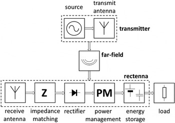
Fig. 1. Far-field radiative WPT system.
The radiated fields of a transmitter are picked up in the far-field region of the transmit antenna by a receive antenna. This signal is rectified, processed (voltage boost converted), and stored in a capacitor or battery. From this capacitor or battery an application (load) is being powered. The dashed box on the receiving side is the rectenna. When the transmitter is unintentional (e.g. a digital television broadcasting station or a base station for the global system of mobile communication), we specify the WPT as RF power harvesting.
In applying far-field radiative WPT, we want to realize power over a large distance. We will be using frequencies in the license-free bands for Industry, Science, and Medicine (ISM) that are limited in allowed transmit powers. Due to this transmit power limitation and the spherical spreading of the transmitted waves, the power density at the receiving antenna will be very low. To keep the PCE, i.e. the ratio of dc output power delivered to the load to the RF input power at the clamps of the receive antenna, as high as possible, all subcomponents of the rectenna (see Fig. 1), must be well matched and means must be devised to maximize the voltage at the input of the rectifier, that is, maximize the rectifier's sensitivity.
II. RECTIFIER
Before discussing the rectifier in detail, we will first look at the impedance matching of the rectifier to the receiving antenna, and then look at the sensitivity of the rectifier.
A) Impedance matching and sensitivity
We regard the rectifier as complex impedance that is matched to the antenna by means of a lossless L-network (see Fig. 2) [Reference Visser2]. The antenna is represented by an equivalent source V s with an internal resistance R s .

Fig. 2. Receive antenna matched to the rectifier.
For a maximum power transfer, the antenna is impedance matched to the rectifier through the series impedance jX 2 and the shunt admittance jB 1, the values of which follow from [Reference Visser2]
 $${R_s}\, = \, \displaystyle{{{G_R}} \over {G_R^2 + {{\lpar {B_1} + {B_R}\rpar }^2}}}\comma \;$$
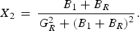 $${X_2}\, = \, \displaystyle{{{B_1} + {B_R}} \over {G_R^2 + {{\lpar {B_1} + {B_R}\rpar }^2}}}.$$
The voltage at the input of the rectifier V R is given, in terms of the rectifier impedance Z R = R R + jX R = 1/(G R + jB R ) [Reference Visser2] as
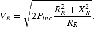 $${V_R} = \sqrt {2{P_{inc}} \displaystyle{{R_R^2 + X_R^2 } \over {{R_R}}}}.$$
To increase the rectenna's PCE we need to increase the rectifier's sensitivity, i.e. increase V R . From equation (3) we conclude that if the rectifier is dominantly resistive (R R ≫ |X R |) we can increase V R by increasing R R and decreasing |X R |. That is, if we have the freedom in tuning R R and X R in designing the rectifier. If the rectifier is dominantly reactive (|X R | ≫ R R ), we should increase |X R | and decrease R R .
B) Rectifier impedance
We use commercially available Schottky diodes in our rectennas in SOT-23 packages containing two diodes and use them in a voltage doubler configuration [3]. Unless we know beforehand that the load (see Fig. 1) will be low-ohmic, we cannot obtain the rectifier's input impedance from an analysis or measurement of a short-circuited diode [Reference Visser, Vullers, Op het Veld and Pop3, Reference Visser and Vullers4] or diode pair [Reference Keyrouz5]. In general, we need to take the load into account in the analysis. Figure 3 shows the real and imaginary parts of a voltage doubler's input impedance as simulated using ADS Harmonic Balance simulator for a load resistor of 10 MΩ and a maximum available input power P in of −10 dBm [Reference Keyrouz5]. The specific application in mind is the capacitively loaded rectenna that is described in [Reference Stoopman, Keyrouz, Visser, Philips and Serdijn6].

Fig. 3. Simulated real and imaginary parts of the input impedance as a function of frequency of an AVAGO HSMS2852-based voltage doubler loaded with a 10 MΩ resistor for a maximum available input power of −10 dBm.
P inc (see Fig. 2) is the actual power at the input of the rectifier or the rectifier preceded by an impedance matching network. P in is the maximum available input power that can be delivered by a source having a 50 Ω internal resistor. In general, P inc ⩽ P in .
We do see that over the frequency range shown the ratio of R over |X| is fairly constant (approximately 0.040) and that |X| highly dominates R.
The available ISM frequency bands and limits on the allowed effective isotropic radiated power (EIRP) (see [Reference Visser and Vullers4]) make the frequency bands around 868 MHz (Europe) and/or 900 MHz (North America) an optimum choice for dedicated far-field radiative WPT and explains our choice for the frequency band as shown in Fig. 3.
The AVAGO HSMS-2852 diode type is selected based on the highest available saturation current, leading to the highest possible dc output voltage. For this Schottky diode, the saturation current is 3 µA [7].
Figure 4 shows the simulated real and imaginary parts of the input impedance of the same voltage doubler as a function of available input RF power for a fixed frequency of 868 MHz.

Fig. 4. Simulated real and imaginary parts of the input impedance as a function of maximum available input power of an AVAGO HSMS2852-based voltage doubler loaded with a 10 MΩ resistor for a fixed frequency of 868 MHz.
Moreover, we observe an input impedance where the reactive part highly dominates the resistive part. We have already found that this is a prerequisite for a high-input voltage and high-power conversion efficiency. Although the impedance is not constant over the shown the maximum available input power range, the impedance mismatch is not severely degraded for low-power levels. This is illustrated in Fig. 5, where the amplitude of the power wave reflection coefficient [Reference Rahola8] is shown as a function of the maximum available input power for the rectifier matched to an impedance of 7.1 + j239.9 Ω.
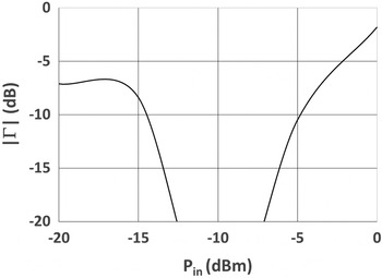
Fig. 5. Amplitude of the power wave reflection coefficient for the rectifier analyzed in Fig. 4, matched for P in =− 10 dBm.
Hence, for a small-band application around the ISM frequency of 868 MHz for the maximum available input power levels ranging from approximately −20 to 0 dBm, we may expect to be able to realize a highly sensitive and power conversion efficient rectenna since the reactive part of the input impedance highly dominates the real part. This has been demonstrated in [Reference Stoopman, Keyrouz, Visser, Philips and Serdijn6] for a high-ohmic load. Now we need to validate this for smaller load resistance values.
III. RECTENNA DESIGN
Having chosen the type of Schottky diode (that we will use in a voltage-doubling configuration), the frequency of operation and the anticipated power levels, we need to connect this rectifier to an antenna. We may use a standard 50 Ω antenna or we may design an antenna that is, conjugate impedance matched to the rectifier. We will compare both situations in this section.
A) 50 Ω Antenna
For the first rectenna prototype we used a broadband, printed Yagi-Uda-like antenna having a 50 Ω input impedance [Reference Keyrouz, Perotto, Visser and Tijhuis9]. The antenna needs to be matched to the Avago HSMS-285X-based voltage doubler for input power levels below −10 dBm at a frequency of 868 MHz. The RF input impedance of the rectifier under these conditions is Z R = 7.1 − j239.9 Ω. A lumped element circuit, as shown in Fig. 2 is used to match the antenna to the rectifier. It consists of a series inductance of 32 nH and a parallel capacitor of 1 pF. The dimensions of the antenna are given in the caption [Reference Keyrouz and Visser10]. Thus, the created rectenna, consisting of a receive antenna, matching network and rectifier is shown in Fig. 6.

Fig. 6. Rectenna, consisting of a 50 Ω receive antenna, a lumped element matching network, and a voltage-doubling rectifier. DL = 106 mm, DW = 8 mm, DD = 8 mm, RL = 167 mm, RW = 5 mm, RD = 20 mm, FL = 158 mm, FW = 10 mm, t = 39 mm, b = 2 mm, and g = 1 mm. The copper thickness is 70 µm. The FR4 board (ε r = 4.28, tanδ = 0.0016) is 1.6 mm thick.
B) Complex conjugate impedance matched antenna
Instead of using a lumped element matching network that occupies space and introduces losses, we can also perform the impedance matching with the antenna structure itself. If we use an antenna structure with enough geometrical features, we should be able to tune the input impedance without much compromising the radiation characteristics [Reference Visser11].
An interesting aspect of the complex conjugate impedance matching is that the real part of the desired antenna impedance is very low, Re{Z A } = 7.1 Ω. To realize such a low resistance we must use an electrically small antenna. To realize the required inductive part of the impedance, Im{Z A } = +239.9 Ω, we must use a loop antenna. Hence, we need a small loop antenna with means to tune the real and imaginary parts of the input impedance. Moreover, we must ensure that the minimization of the antenna does not lead to unacceptable low radiation efficiency.
These considerations have led to a printed rectangular loop with additional short-circuiting arms as shown in Fig. 7 [Reference Keyrouz5].

Fig. 7. Rectangular loop-like antenna with additional short-circuiting arms, printed on a dielectric carrier.
The radiation efficiency is controlled by the length L 1 of the rectangular loop. By adding the horizontal arms, the complex input impedance of the antenna may be tuned. The impedance versus frequency trend behavior may be modeled by regarding this antenna as a small folded dipole antenna and decomposing the current in a dipole mode current and a short-circuited stub transmission line mode current as used in [Reference Visser12] for resonant folded dipole antennas. For a more accurate impedance calculation, we have to resort to full-wave analysis, e.g. CST Microwave Studio®.
Fig. 8 shows the surface current densities for four loop-like antennas, evaluated at 868 MHz [Reference Keyrouz5]. The dimensions, referring to Fig. 6, are stated in the figure caption.
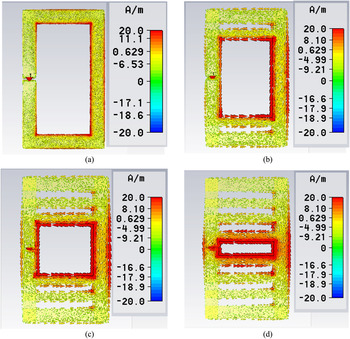
Fig. 8. Simulated current density at 868 MHz for four loop-like antennas, denoted A1, A2, A3, and A4.
Figure 9 shows the impedance and radiation efficiency of all the antennas as a function of frequency.
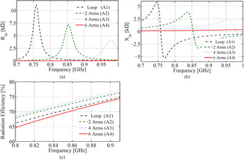
Fig. 9. Real part of the input impedance (a), imaginary part of the input impedance (b), and radiation efficiency (c) as a function of frequency for the antennas shown in Fig. 8.
With the antenna for which the current density is shown in Fig. 8(d) we are able to conjugately match to the HSMS2852-based voltage doubler rectifier. The antenna connected to the rectifier is shown in Fig. 10.

Fig. 10. Realized rectenna consisting of a printed loop-like antenna directly connected to a voltage doubler rectifier.
IV. RESULTS
To characterize both rectenna prototypes we have made use of the setups as shown in Fig. For both rectenna characterizations we make use of the same transmitter, operating at the same frequency and using the same EIRP levels. At the receiver side, we start using a 50 Ω receive antenna that is identical to the antenna used in the 50 Ω rectenna (Fig. 6) and connect it to a power meter, as shown in Fig. 11(a). With the EIRP levels and R known, the Friis equation is used to validate the simulated value of the receive antenna gain G 50 to record the power at the input of the impedance matching network P in,50, as shown in Fig. 11(a). The difference between the calculated and the measured power appear to be within ±0.5 dB and is attributed for not being in a real free-space environment.
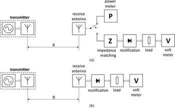
Fig. 11. Rectenna measurement setups. (a) Setup for 50 Ω rectenna measurement. (b) Setup for complex conjugate impedance matched rectenna measurement.
Next the voltages V L over different resistive loads R L are measured and the RF-to-dc PCE is calculated as
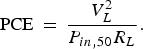 $${\rm PCE}\, = \, \displaystyle{{V_L^2 } \over {P_{in\comma 50} R_L }}.$$
For the characterization of the complex conjugately impedance matched rectenna, we have used the setup as shown in Fig. 11(b), using the same transmitter, distance R, and EIRP levels as in the setup shown in Fig. 11(a). The input power at the rectifier P in,cm has been determined from the previously found gain of the 50 Ω antenna and the simulated gain of the rectangular loop-like antenna (see Fig. 7) G cm , according to
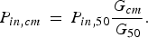 $$P_{in\comma cm} \, = \, P_{in\comma 50} \displaystyle{{G_{cm} } \over {G_{50} }}. $$
Although the simulated gain has not been verified by measurements, we have verified the simulated radiation efficiency by Wheeler cap measurements and have obtained the results having a relative difference below 5%.
The results of the narrow band characterization compared with the state of the art for the 50 Ω rectenna is shown in Table 1. We have only compared with the systems working in the same frequency range and showing similar PCE values. The optimum load resistor values in our work have been obtained through experiments. The efficiency is determined relative to the maximum available power – as is typically done in literature – and not to the actual power at the input of the rectifier which is smaller (reflection coefficient is −5.6 dB).
Table 1. Measured performances and comparison with state of the art for the 50 Ω rectenna shown in Fig. 6
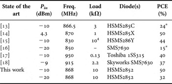
*Obtained from graphs.
The results show a distinct improvement in PCE compared with the state of the art. The optimum load resistance value of our rectenna (10 kΩ) is compatible with the input impedance of commercially available power management circuits (e.g. [19]), which may boost a 100 mV up to any value below 4.2 V.
In [Reference De Donno, Catarinucci and Tarricone13] and [Reference Kanaya, Tsukamaoto, Hirabaru and Kanemoto15] a four-diode rectifier has been employed. In [Reference Monti, Corchia and Tarricone14] and [Reference Georgiadis, Collado, Via and Menses16] a single diode has been used.
A further improvement, both in PCE and in size is realized with the rectenna as shown in Fig. 10. The results, compared with the state-of-the-art results are shown in Table 2. Due to the gain inaccuracy mentioned earlier, the efficiencies have an error margin of ±10 %.
Table 2. Measured performances and comparison with state of the art for the complex conjugate impedance matched rectenna shown in Fig. 10.

The results show an improvement of PCE and size with respect to the state of the art.
IV. CONCLUSION
We have shown earlier that for realizing a small-size rectenna with an optimum RF-to-dc PCE, the following measures should be taken:
-
– Impedance match the antenna to the rectifier;
-
– Opt for a rectifier having a dominant reactive input impedance;
-
– Directly match the antenna to the rectifier using complex conjugate matching;
-
– Miniaturize the antenna to realize the desired impedance.
Using these design rules we were able to obtain a PCE of 55% at an input power level of −10 dBm at 868 MHz. This is a significant improvement over the reported state of the art.
 Hubregt J. Visser received the M.Sc. degree in Electrical Engineering from Eindhoven University of Technology (TU/e), The Netherlands, in 1989. In 1990, he joined TNO Physics and Electronics Laboratory, The Hague, The Netherlands. He has participated in several projects concerning near-field antenna measurements, monolithic microwave integrated circuits design, and phased-array antenna design. In 2001 he joined TNO Science and Industry, Eindhoven, The Netherlands where he has been involved in antenna miniaturization projects. In 2009, he joined the Holst Centre as an employee of Imec working on wireless energy transfer. In 2009, he obtained a Ph.D. degree from Eindhoven University of Technology, The Netherlands and Katholieke Universiteit Leuven, Belgium. In 2014, he was appointed as professor at TU/e. Hubregt is the author of the books “Array and Phased Array Antenna Basics” (Wiley, 2005), “Approximate Antenna Analysis for CAD” (Wiley, 2009), and ‘Antenna Theory and Applications’ (Wiley, 2012).
 Shady Keyrouz received the B.Sc. degree in Electrical Engineering from Notre Dame University in Beirut, Lebanon, in 2008. He received the M.Sc. degree in Communication Technology from Ulm University in Germany, in 2010 and the Ph.D. degree from Eindhoven University of Technology, The Netherlands, in 2014. His research interests include antenna modeling, rectenna design, wireless power transmission, and reflect-array antennas.
 Bart Smolders received his M.Sc. and Ph.D. degree in Electrical Engineering from the Eindhoven University of Technology (TU/e), The Netherlands, in 1989 and 1994, respectively. From 1989 to 1991, he worked as an IC Designer at FEL-TNO, The Hague, The Netherlands. From 1994 to 1997, he was a Radar System Designer with Thales, The Netherlands. From 1997 to 2000, he was the project leader of the Square Kilometer Array (SKA) with the Netherlands Foundation for Research in Astronomy (ASTRON). From 2000 to 2010, he has been with NXP (formerly Philips) Semiconductors, The Netherlands, responsible for the innovation in the RF business line. In 2007, he was appointed as professor at TU/e in the Electromagnetics Group with special interest in antenna systems and applications. He is the Chairman of the NERG (Nederlands Radio- en Elektronica Genootschap), Vice-chair of IEEE-Benelux, and Vice-chair of the EuCAP 2014 Organizing Committee.


