The remarkable properties of two-dimensional (2D) materials hold tremendous potential for next-generation electronic and optoelectronic applications. For example, the low defect densities and high carrier mobilities of 2D single-crystal organic semiconductors could enhance performance in flexible electronics. Likewise, graphene’s high conductivity and optical transparency make it an attractive candidate for electrodes.
In these and other areas of 2D materials research, characterizing crystallinity is often fundamental. Knowing the lattice structure verifies that the desired crystal was produced and helps evaluate the synthesis process. Such measurements have traditionally been considered the domain of high-resolution transmission electron microscopy (HRTEM) or low-temperature, ultrahigh-vacuum scanning tunneling microscopy (LT-UHV STM). Both techniques provide sufficient resolution to visualize the crystal structure and determine characteristics such as symmetry, orientation, and lattice constants.
Imaging the atomic lattice of 2D crystals is also possible with some of today’s commercial atomic force microscopes (AFMs), such as the Cypher. Spatial resolutions comparable to—or even better than—HRTEM’s current limit Reference Kisielowski, Freitag, Bischoff, van Lin, Lazar, Knippels, Tiemeijer, van der Stam, von Harrach, Stekelenburg, Haider, Uhlemann, Müller, Hartel, Kabius, Miller, Petrov, Olson, Donchev, Kenik, Lupini, Bentley, Pennycook, Anderson, Minor, Schmid, Duden, Radmilovic, Ramasse, Watanabe, Erni, Stach, Denes and Dahmen1 of ∼50 pm can now be achieved routinely, thanks to instrumentation improvements. Regions of 2D materials with local atomic flatness, in particular, present optimal conditions for high-resolution AFM imaging, since they allow fewer atoms (or even a single atom) in the tip to interact with the surface. AFMs also have the practical advantages of operating under ambient conditions and on both conducting and insulating samples.
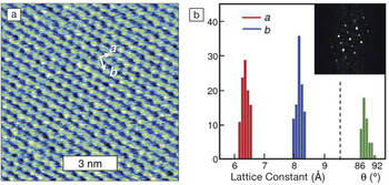
These concepts are demonstrated in Figure 1 , which shows results for a bilayer of the organic semiconductor crystal dioctylbenzothienobenzothiophene (C8-BTBT) formed by a floating-coffee-ring-driven assembly. Reference Wang, Qian, Li, Zhang, He, Jiang, Wang, Wang, Pan, Wang, Wang, Hu, Nan, Ni, Zheng and Shi2 C8-BTBT was dissolved in a mixture of solvent and antisolvent, and the solution was dropcast on a silicon/silicon oxide substrate. Airflow allowed the drop to be dragged rapidly across the surface, and the evaporation-driven flow of the solvent enabled 2D crystallization precisely at the solvent/antisolvent interface. Although Figure 1a was acquired in tapping mode using the amplitude signal, images can also be obtained in either tapping or contact mode with the height (Z-sensor) signal. Lattice constant measurements may then be made from either the image directly or its spatial Fourier transform (FFT).

Figure 1. (a) Image of a dioctylbenzothienobenzothiophene (C8-BTBT) bilayer acquired with the amplitude signal in tapping mode. Vectors indicate the oblique unit cell with lattice constants a and b. (b) Histograms of a, b, and angle θ obtained from analysis of 10 images acquired at different places on the bilayer. The inset shows the Fourier transform of (a) with full width 12 nm–1. Adapted from Reference 2.
Similarly, ultrahigh-resolution imaging can be performed on other 2D materials. Figure 2 shows graphene grown by high-temperature molecular beam epitaxy. Reference Summerfield, Davies, Cheng, Korolkov, Cho, Mellor, Foxon, Khlobystov, Watanabe, Taniguchi, Eaves, Novikov and Beton3 In Figure 2a, two regions of graphene, separated by a central crack, display hexagonal moiré patterns that arise from lattice mismatch between the graphene and the hexagonal boron nitride (hBN) substrate. Defects and variable periodicity in the moiré patterns represent strain-induced spatial variations in the graphene lattice constant. In the smaller-scale images in Figure 2b–d, the vectors indicate that both graphene regions (Figure 2b and d) have the same lattice orientation and are aligned with the hBN substrate (Figure 2c).

Figure 2. (a) Topography image of epitaxial graphene on hexagonal boron nitride.
(b–d) Lattice-resolution topography images acquired within the square regions indicated in (a). The scan size of each image is 5 nm. All images acquired in contact mode in air. Adapted from Reference 3; images courtesy of A. Summerfield, V. Korolkov, and P. Beton, The University of Nottingham.
The impressive spatial resolution in these images was achieved through the instrument design of Cypher AFMs. In the lateral direction, closed-loop control provides more accurate XY scanning than the open-loop operation of older AFMs. Use of symmetric design, thermally stable materials, and smaller enclosures has reduced additional scanning distortion due to thermal drift. In the vertical direction, Cypher’s noise floor has been lowered to <15 pm, in part by making the mechanical loop between the tip and sample as short and stiff as possible. Even for the highest resolution imaging, Cypher AFMs do not require extra vibration isolation equipment in most labs.
An additional factor in attaining higher spatial resolution is the use of smaller cantilevers (<10 µm long), which have intrinsically lower thermal noise for the same spring constant. To accommodate small cantilevers and enable faster scanning, the Cypher AFM has a smaller laser spot size (3 × 9 μm2), faster control electronics, and higher instrument resonances than older AFMs. These improvements enable Cypher to scan 10–100× faster than conventional AFMs, meaning a complete 256 × 256 pixel image can be acquired in just seconds.
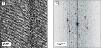
Images resolving the atomic lattice can also be obtained by measuring the cantilever’s lateral deflection in contact mode. Reference Marsden, Phillips and Wilson4 This approach is called lateral force microscopy (LFM), or friction force microscopy (FFM) if the difference between trace and retrace signals is used. Image contrast in LFM and FFM arises from periodic slip-stick of atomic-scale frictional forces. These techniques are particularly useful for samples fabricated on rougher substrates because the contrast is largely independent of topography. For example, Figure 3 shows a LFM image acquired on graphene grown by low-pressure chemical vapor deposition on copper foil. Reference Marsden, Phillips and Wilson4 The spatial FFT clearly shows graphene’s characteristic hexagonal arrangement of peaks and enables local lattice orientation to be determined. By collecting more than 1000 such images unattended for more than seven hours, the grain orientation map of a 25 × 25 μm2 sample region was obtained.

Figure 3. (a) Lattice-resolution image of graphene on copper foil obtained with lateral force microscopy in air. (b) Fourier transform of a larger image (scan size 20 nm) from which the image in (a) was extracted. The red dashed lines highlight a hexagonal pattern of peaks indicative of crystalline graphene. Adapted from Reference 4.
These results demonstrate how ongoing improvements to fundamental performance have enabled modern AFMs to provide useful characterization of the crystal structure of 2D materials. Multiple research groups worldwide now routinely use Cypher AFMs to reveal details that were once in the exclusive domain of techniques such as HRTEM and LT-UHV STM. Together with advances in quantitative measurements of electrical, mechanical, and functional properties, these capabilities make AFMs more valuable than ever for 2D materials research.
Cypher AFMs are available exclusively from Oxford Instruments Asylum Research. For more information, visit www.oxford-instruments.com/afm-webinars to view recorded webinars on AFM characterization of 2D materials, as well as technical advances in Cypher AFMs.


