A new study published in Nature Materials (doi:10.1038/s41563-018-0154-x) offers key insights into the formation of layered two-dimensional (2D) perovskite films known as Ruddlesden–Popper phases, a class of materials that hold promise for stable light-harvesting and -emitting devices.
Despite being one of the most attractive materials for photovoltaics and light-emitting devices, conventional three-dimensional organic–inorganic perovskites are plagued by instability issues. However, their 2D counterparts, which contain layers of conductive perovskites separated by layers of relatively long organic cations, are much more stable. The cations inhibit charge transport between neighboring conductive inorganic layers. This forms quantum wells, where the charge carriers can freely move in a 2D space, while there is a restriction in the third dimension.
So far, though, not much is understood about their composition or how these materials assemble. To investigate, Edward Sargent and colleagues at the University of Toronto used grazing incidence x-ray scattering on 2D layered perovskite films as the films formed.
They used methylammonium lead iodide with either phenethylammonium or n-butylammonium cations, and different solvents to make various film samples. They found that intermediate solvent complexes mediated the formation of quantum wells by providing building blocks to grow perovskites as the solvent evaporates out. They also found that changing the cation changed the well distribution.
This understanding could help control the distribution, composition, and orientation of 2D layered perovskites, properties that influence device performance. The results could be applied to any such material. “This work paves the way toward engineering higher quality materials for more efficient and stable optoelectronic devices,” the researchers say.
The layered nature of Ruddlesden–Popper perovskites means that the materials can be shaved down to a single layer or just a few layers. The properties of any material at the molecular level are different from those at larger scales. Kian Ping Loh, at the National University of Singapore, and his colleagues have revealed what makes the properties of 2D perovskites differ at molecularly thin dimensions. Their work appears in the journal Nature Materials (doi:10.1038/s41563-018-0164-8).

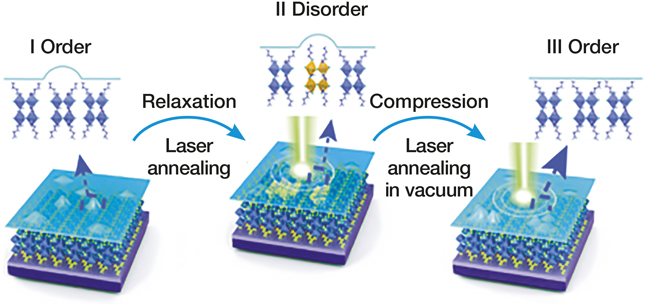
Schematic diagram showing the order–disorder transition by laser illumination. Credit: Nature Materials.
The researchers made centimeter-sized crystals of the perovskite (CH3(CH2)3NH3)2(CH3NH3)n–1PbnI3n+1 (n = 1, 2, 3, 4 ) and exfoliated 20–100-µm-thick monolayer sheets from the material. They measured the optical properties of the bulk and monolayer flakes using photoluminescence and optical absorption measurements. To keep the flakes from decomposing under laser irradiation used for these studies, they encapsulated the flakes with a transparent 2D hexagonal boron nitride layer.
The researchers studied the photoresponsivity of the single-crystal 2D perovskites as a function of thickness and discovered that excitons—joint states of an electron and a positively charged hole—tunnel across the material interlayers to dissociate at the electrodes, leading to efficient photocurrent generation. As n increased, the luminescence of the materials shifted toward longer, redder wavelengths. The redshift also happened when the material was exposed to the laser for a long time, because thermal fluctuations reoriented the surface organic cations in the monolayer perovskite. The color shift can be reversed by exposing the sample to higher power laser annealing under vacuum. This cycle could be repeated tens of times.
The disordering of the organic cations also creates defects that trap only positively charged carriers, allowing electrons to circulate longer. To test this, the researchers made a photodetector with the monolayer perovskites. The detector had a low current in the dark. But the current increased linearly with laser power because under illumination, excitons tunneled across the interlayers, creating a highly conductive state.
Concentrated photovoltaic (CPV) devices, which use lenses and mirrors to focus sunlight onto small, highly efficient solar cells, can have power-conversion efficiencies as high as 46%. Very expensive multi-junction solar cells made with III–V semiconductors, such as gallium indium phosphide, are often used for such devices.
Could perovskite solar cells, which suffer from instability under light and heat, be used for CPV technology? University of Oxford researchers led by Henry Snaith answer that question in a study published in Nature Energy (doi:10.1038/s41560-018-0220-2). They found that the efficiency of halide perovskite solar cells went up from 21.1% to a peak of 23.6% when simulated sunlight was increased to 14 times the standard irradiance of 1 Sun.
The researchers assessed a range of perovskite materials for their stability under high-intensity light. Perovskites containing a mixed cation formamidinium-cesium composition gave the most stable solar cells under high irradiance, and they chose Fa0.83Cs0.17PbI2.7Br0.3 for the CPV device. They found that their devices, maintained at room temperature during operation, retained 90% of their original efficiency after 150 hours spent under 10 Suns of concentrated light.


