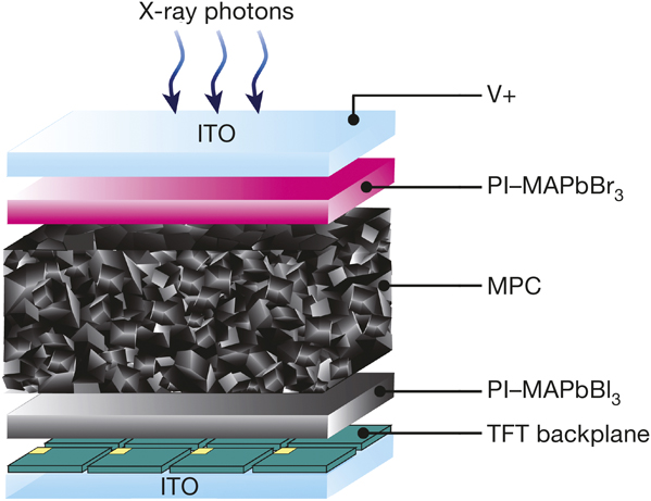
In an advance that could herald one of the first commercial applications for perovskites, South Korean researchers have printed thick perovskite layers that can be used as x-ray detectors. The detectors, reported in the journal Nature (doi:10.1038/nature24032), could produce sharper medical images at lower x-ray doses. They would also be cheaper to make than today’s flat x-ray detectors.
Flat detectors use one of two methods to convert x-ray energy to electrons. The indirect conversion method uses luminescent cesium iodide on a silicon photodetector array. The direct method, based on amorphous selenium photoconductors, creates sharper images and is used for low-energy mammography. But amorphous selenium cannot absorb higher-energy x-rays that are needed for general imaging.
Organic–inorganic perovskites are ideal photoconductors because they are 10 times more sensitive to x-rays than amorphous selenium. The challenge has been to make perovskite layers that are thick and large enough: photodetectors are hundreds of micro-meters thick and 50 cm × 50 cm in size.

Illustration of an all-solution-processed digital x-ray detector. ITO, indium tin oxide; PI, polyimide; MPC, MAPbI3 photoconductor; TFT, thin-film transistor. Credit: Nature.
The team from the Samsung Advanced Institute of Technology and Sungkyunkwan University made a dense, viscous solution of CH3NH3I and PbI2 in γ-butyrolactone and α-terpineol, and used a doctor blade to print an 830-µm-thick CH3NH3PbI3 perovskite layer. Then they made an x-ray detector array using a 10 cm × 10 cm sample of the perovskite.
High-efficiency perovskite solar cells have, to date, been made mostly with either spiro-OMeTAD or poly(triarylamine) as the hole-extracting material. But both are prohibitively expensive for large-scale use. Researchers have now made stable perovskite solar cells with efficiencies of more than 20% by using low-cost copper thiocyanate (CuSCN) as the hole-transporting layer.
CuSCN is an attractive hole-transport material since it is a cheap p-type semiconductor that efficiently transports holes. But most solvents it dissolves in can damage the underlying perovskite layer.
Researchers from École Polytechnique Fédérale de Lausanne deposited CuSCN dissolved in diethyl sulfide solvent while spinning the substrate at 5000 rpm to quickly evaporate the solvent. They also added a conductive reduced graphene oxide layer between the CuSCN and gold contact, which led to excellent operational stability under full-sun illumination at 60°C.
The resulting solar cells retained more than 95% of their efficiency after 1000 hours, surpassing the stability of spiro-OMeTAD devices. The results are reported in the journal Science (doi: 10.1126/science.aam5655).
To make perovskite solar cells commercially, manufacturers will need to produce high-quality perovskites on large areas for a low cost. The challenge is that scaling up small laboratory devices to more than 25 cm2 can reduce the power-conversion efficiency anywhere from 10 to 20%.
Researchers from Shanghai Jiao Tong University in China have come up with an easy route to making uniform, defect-free, large-area perovskite films in air at room temperature. The process does not require conventional solvents and a vacuum. As reported in the journal Nature (doi:10.1038/nature23877), researchers made 36 cm2 solar cells that were more than 12% efficient. The researchers placed a 1:1 mixture of the amine complex precursors CH3NH3I3•CH3NH2 and PbI2•CH3NH2 on a substrate, applied a smooth polyimide film on top, pressed down on it for a minute with a squeezing board to spread the liquid, and then warmed the substrate at 50°C for two minutes. When they peeled off the polyimide film, a dense, uniform perovskite film had formed.
Perovskites’ low stability and lead toxicity remain hurdles to commercial use. Double perovskites are an appealing alternative. Now researchers have, for the first time, made double perovskite films and built a working solar cell from the film.
Conventional perovskites have the formula ABX3. Double perovskites, in which the unit cell is twice that of a conventional perovskite, have the formula AB′B″X6.
The double perovskite Cs2AgBiX6 (X = Cl, Br) is a promising material for solar cells since it is less toxic and stable. However, its precursor’s low solubility has so far hampered the fabrication of high-quality films.
The team from the University of Munich, Germany, and Newcastle University, UK, found that annealing at more than 250°C was key for converting the precursors into high-quality perovskite films. They made Cs2AgBiBr6 films by dissolving BiBr3, AgBr, and CsBr in dimethylsulfoxide; preheating the solution to 75°C, and then spin-coating it onto a substrate that was subsequently annealed at 285°C.
Photovoltaic devices made with the films have a power-conversion efficiency of up to 2.43%, an open-circuit voltage of more than 1 V, and a high stability under operating conditions, the researchers reported in the Journal of Materials Chemistry A (doi:0.1039/c7ta06816f).


