Hostname: page-component-586b7cd67f-t7czq Total loading time: 0 Render date: 2024-11-26T19:47:20.797Z Has data issue: false hasContentIssue false

Correlation Between Nanoscale Structural, Electronic, and Magnetic Properties of Thin Films by Scanning-Probe Microscopy and Spectroscopy

Published online by Cambridge University Press:  29 November 2013

Get access

Extract

Heteroepitaxial pseudomorphic thin-film growth allows the stabilization of solids in structures—that is, with crystalline symmetries and lattice constants that are far from those of the corresponding bulk material. This facilitates the tailoring of materials properties that do not exist in nature. Usually a strong correlation is found between the atomic, electronic, and magnetic structure of thin films, which leads to a drastic dependence of their physical properties on the details of growth conditions such as substrate temperature, evaporation rate, and background pressure. To learn more about the fundamental relationship between structural, electronic, and magnetic properties of thin films as well as to improve the reproducibility of their physical properties in view of technical applications, it is mandatory to apply experimental techniques with sufficient, ultimately atomic spatial resolution combined with high sensitivity. The class of scanning-probe microscopies and spectroscopies is ideally suited for that purpose as schematically illustrated in Figure 1. Scanning tunneling spectroscopy (STS) establishes the correlation between atomic structure and local electronic properties, while spin-polarized scanning tunneling spectroscopy (SPSTS) relates local electronic and magnetic properties. Additionally the correlation
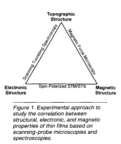
between topographical and magnetic structure can be addressed by magnetic force microscopy (MFM) though the spatial resolution is limited to about 10–50 nm. Since magnetic thin films are usually sensitive to oxidation, their preparation and characterization have to be performed in situ under ultrahigh vacuum (UHV) conditions in order to achieve reproducible experimental conditions. While STS is now routinely applied in UHV, it has only been recently that the first MFM studies under UHV conditions have been reported. In the following, representative examples of the application of STS, SPSTS, and MFM in ultrathin Fe, Gd, and Co films will be presented.

Type
Nanoscale Characterization of Materials
Copyright
Copyright © Materials Research Society 1997

Access options

Get access to the full version of this content by using one of the access options below. (Log in options will check for institutional or personal access. Content may require purchase if you do not have access.)

References

1.Wiesendanger, R., in Scanning Probe Microscopy and Spectroscopy: Methods and Applications (Cambridge University Press, Cambridge, 1994).CrossRefGoogle Scholar
2.Hamers, R.J., in Scanning Tunneling Microscopy I, edited by Güntherodt, H-J. and Wiesendanger, R. (Springer Ser. in Surface Sciences, 2nd ed., Springer-Verlag, Berlin, Heidelberg, New York, 1994).Google Scholar
3.Wiesendanger, R., in Handbook of Microscopy, edited by Amelinckx, S., van Dyck, D., van Landuyt, J., and van Tendoloo, G. (VCH, Weinheim, 1997).Google Scholar
4.Wiesendanger, R., J. Magn. Soc. Jpn. 18 (1994) p. 4.Google Scholar
5.Wiesendanger, R., in Analytical Methods in Scanning Probe Microscopy, edited by Wiesendanger, R. (Springer-Verlag, Berlin, Heidelberg, New York) in press.Google Scholar
6.Grütter, P., Mamin, H.J., and Rugar, D., in Scanning Tunneling Microscopy II, edited by Wiesendanger, R. and Güntherodt, H-J., Springer Ser. in Surface Sciences (Springer-Verlag, Berlin, Heidelberg, New York, 2nd ed., 1995).Google Scholar
7.Wadas, A., in Handbook of Microscopy, edited by Amelinckx, S., van Dyck, D., van Landuyt, J., and van Tendeloo, G. (VCH, Weinheim, 1997).Google Scholar
8.Wadas, A., Löhndorf, M., Dreyer, M., and Wiesendanger, R., Appl. Phys. A64 (1997) p. 353.CrossRefGoogle Scholar
9.Jensen, C., Reshöft, K., and Köhler, U., Appl. Phys. 62 (1996) p. 217.Google Scholar
10.Bode, M., Pascal, R., and Wiesendanger, R., Appl. Phys. 62 (1996) p. 571.CrossRefGoogle Scholar
11.Wiesendanger, R., Bode, M., Pascal, R., Allers, W., and Schwarz, U.D., J. Vac. Technol. A 14 (1996) p. 1161.CrossRefGoogle Scholar
12.Heinze, S., Blügel, S., and Wiesendanger, R., (unpublished manuscript).Google Scholar
13.Bode, M., Pascal, R., Dreyer, M., and Wiesendanger, R., Phys. Rev. B 54 (1996) p. R8385.CrossRefGoogle Scholar
14.Kurzawa, R., Kämper, K-P., Schmitt, W., and Güntherodt, G., Solid Commun. 60 (1986) p. 777.CrossRefGoogle Scholar
15.Elmers, H.J., Hauschild, J., Höche, H., Gradmann, U., Bethge, H., Heuer, D., and Köhler, U., Solid Commun. 73 (1994) p. 898.Google Scholar
16.Elmers, H.J., Hauschild, J., Fritzsche, H., Lin, G., Gradmann, U., and Köhler, U., Solid. Commun. 75 (1995) p. 2031.Google Scholar
17.Pascal, R., Zarnitz, Ch., Bode, M., and Wiesendanger, R., Phys. Rev. B 56 (7) (1997).CrossRefGoogle Scholar
18.Pascal, R., Zarnitz, Ch., Bode, M., and Wiesendanger, R., unpublished manuscriptGoogle Scholar
19.Kolaczkiewicz, J. and Bauer, E., Surf. Sci. 175 (1986) p. 487.CrossRefGoogle Scholar
20.Wiesendanger, R., Güntherodt, H-J., Güntherodt, G., Gambino, R.J., and Ruf, R., Phys. Rev. Lett. 65 (1990) p. 247.CrossRefGoogle Scholar
21.Wiesendanger, R., Shvets, I.V., Bürgler, D., Tarrach, G., Güntherodt, H-J., and Coey, J.M.D., Europhys. Lett. 19 (1992) p. 141.CrossRefGoogle Scholar
22.Wiesendanger, R., Bode, M., Kleiber, M., Löhndorf, M., Pascal, R., Wadas, A., and Weiss, D., J. Vac. Sci. Technol. B 15 (4) 1997.Google Scholar
23.Bode, M., Pascal, R., and Wiesendanger, R. (unpublished manuscript).Google Scholar
24.Weber, N., Wagner, K., Elmers, H.J., Hauschild, J., and Gradmann, U. (unpublished manuscript).Google Scholar
25. OMICRON, Taunusstein, Germany.Google Scholar
26.Löhndorf, M., Wadas, A., van den Berg, H.A.M., and Wiesendanger, R., Appl. Phys. Lett. 68 (1996) p. 3635.CrossRefGoogle Scholar