Hostname: page-component-745bb68f8f-v2bm5 Total loading time: 0 Render date: 2025-01-11T09:53:03.789Z Has data issue: false hasContentIssue false

Van der Waals epitaxy and composition control of layered SnSxSe2−x alloy thin films

Published online by Cambridge University Press:  31 January 2020
Joshua J. Fox
Affiliation:
Department of Materials Science and Engineering, The Pennsylvania State University, University Park, Pennsylvania 16802, USA
Xiaotian Zhang
Affiliation:
Department of Materials Science and Engineering, The Pennsylvania State University, University Park, Pennsylvania 16802, USA
Zakaria Y. Al Balushi
Affiliation:
Department of Materials Science and Engineering, The Pennsylvania State University, University Park, Pennsylvania 16802, USA
Mikhail Chubarov
Affiliation:
2D Crystal Consortium-Materials Innovation Platform, The Pennsylvania State University, University Park, Pennsylvania 16802, USA
Azimkhan Kozhakhmetov
Affiliation:
Department of Materials Science and Engineering, The Pennsylvania State University, University Park, Pennsylvania 16802, USA
Joan M. Redwing*
Affiliation:
Department of Materials Science and Engineering, 2D Crystal Consortium-Materials Innovation Platform, The Pennsylvania State University, University Park, Pennsylvania 16802, USA
*
a)Address all correspondence to this author. e-mail: [email protected]
Get access

Abstract

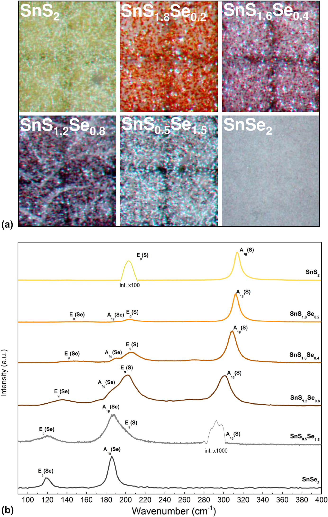
Epitaxial SnSxSe2−x films with tunable band gap energies (1.0–2.2 eV) are of growing interest for photodetectors and 2D heterostructures for nanoscale electronics. In this study, powder vapor transport growth of SnSxSe2−x was investigated on c-plane sapphire and epitaxial graphene (EG)/6H–SiC substrates using tin, sulfur, and selenium powder sources in a heated tube furnace. The SnSxSe2−x composition was controlled by varying the sulfur and selenium source temperatures and the corresponding chalcogen vapor pressure ratio. Raman spectroscopy was used to determine the alloy composition of the films, and the optical properties were characterized using UV-Vis-NIR spectroscopy. SnSxSe2−x grown on sapphire consisted of vertically oriented platelets. By contrast, large-area, planar coalesced SnSxSe2−x films grew on EG with low surface roughness indicative of a van der Waals growth mode. High-resolution X-ray diffraction θ–2θ scans and pole figure analysis confirm that the SnSxSe2−x films are c-axis oriented with epitaxial relation being $\left[ {11\bar{2}0} \right]$ SnSxSe2−x$\left[ {10\bar{1}0} \right]$ 6H–SiC.

Type
Article
Copyright
Copyright © Materials Research Society 2020

Access options

Get access to the full version of this content by using one of the access options below. (Log in options will check for institutional or personal access. Content may require purchase if you do not have access.)

Footnotes

b)

This author was an editor of this journal during the review and decision stage. For the JMR policy on review and publication of manuscripts authored by editors, please refer to http://www.mrs.org/editor-manuscripts/.

References

Ma-Balleste, R., Gomez-Navarro, C., Gomez-Herrero, J., and Zamora, F.: 2D materials: To graphene and beyond. Nanoscale 3, 2030 (2011).CrossRefGoogle Scholar
Mak, K.F. and Shan, J.: Photonics and optoelectronics of 2D semiconductor transition metal dichalcogenides. Nat. Photonics 10, 216226 (2016).CrossRefGoogle Scholar
Huang, Y., Sutter, E., Sadowski, J.T., Cotlet, M., Monti, O.L., Racke, D.A., Neupane, M.R., Wickramaratne, D., Lake, R.K., Parkinson, B.A., and Sutter, P.: Tin disulfide—An emerging layered metal dichalcogenide semiconductor: Materials properties and device characteristics. ACS Nano 8, 1074310755 (2014).CrossRefGoogle ScholarPubMed
Zhou, X., Zhang, Q., Gan, L., Li, H., Jie, X., and Zhai, T.: Booming development of group IV–VI semiconductors: Fresh blood of the 2D family. Adv. Sci. 3, 1600177 (2016).10.1002/advs.201600177CrossRefGoogle ScholarPubMed
Harbec, J.Y., Paquet, Y., and Jandl, S.: Crystallography and temperature dependence of the resistivity of SnS2−xSex solid solutions. Can. J. Phys. 56, 11361139 (1978).CrossRefGoogle Scholar
Gonzalez, J.M. and Oleynik, I.I.: Layer-dependent properties of SnS2 and SnSe2 novel two-dimensional materials. Phys. Rev. B 94, 125443 (2016).CrossRefGoogle Scholar
Domingo, G., Itoga, R.S., and Kannewurf, C.R.: Fundamental optical absorption in SnS2 and SnSe2. Phys. Rev. 143, 536541 (1966).CrossRefGoogle Scholar
Fan, C., Li, Y., Lu, F., Deng, H-X., Wei, Z., and Li, J.: Wavelength dependent UV-Vis photodetectors from SnS2 flakes. RSC Adv. 6, 422427 (2016).CrossRefGoogle Scholar
Zhou, X., Gan, L., Tian, W., Zhang, Q., Jin, S., Li, H., Bando, Y., Golberg, D., and Zhai, T.: Ultrathin SnSe2 flakes grown by chemical vapor deposition for high-performance photodetectors. Adv. Mater. 27, 80358041 (2015).CrossRefGoogle ScholarPubMed
Zhou, X., Zhang, Q., Gan, L., Li, H., and Zhai, T.: Large-size growth of ultrahin SnS2 nanosheets and high performance for phototransistors. Adv. Funct. Mater. 26, 44054413 (2016).CrossRefGoogle Scholar
Yang, D., Li, B., Hu, C., Deng, H., Dong, D., Yang, X., Qiao, K., Yuan, S., and Song, H.: Controllable growth orientation of SnS2 flakes for low-noise, high-photoswitching ratio, and ultrafast phototransistors. Adv. Opt. Mater. 4, 419426 (2015).10.1002/adom.201500506CrossRefGoogle Scholar
Liu, G., Li, Z., Hasan, T., Chen, X., Zhang, W., Feng, W., Jia, D., Zhou, Y., and Hu, P.: Vertically aligned two-dimensional SnS2 nanosheets with a strong photon capturing capability for efficient photoelectrochemical water splitting. J. Mater. Chem. A 5, 19891995 (2016).CrossRefGoogle Scholar
Song, H.S., Li, S.L., Gao, L., Xu, Y., Ueno, K., Tang, J., Cheng, Y.B., and Tsukagoshi, K.: High-performance top-gated monolayer SnS2 field-effect transistors and their integrated logic circuits. Nanoscale 5, 96669670 (2013).10.1039/c3nr01899gCrossRefGoogle ScholarPubMed
Pei, T., Bao, L., Wang, G., Ma, R., Yang, H., Li, J., Gu, C., Pantelides, S., Du, S., and Gao, H-J.: Few-layer SnSe2 transistors with high on/off ratios. Appl. Phys. Lett. 108, 053506 (2016).10.1063/1.4941394CrossRefGoogle Scholar
Pan, T.S., De, D., Manongdo, J., Guloy, A.M., Hadjiev, V.G., Lin, Y., and Peng, H.B.: Field effect transistors with layered two-dimensional SnS2−xSex conduction channels: Effects of selenium substitution. Appl. Phys. Lett. 103, 093108 (2013).CrossRefGoogle Scholar
Yan, X., Lie, C., Li, C., Bao, W., Ding, S., and Zhang, D.: Tunable SnSe2/WSe2 heterostructure tunnelling field effect transistor. Small 13, 1701478 (2017).10.1002/smll.201701478CrossRefGoogle Scholar
Perumal, P., Ulaganathan, R.K., Sankar, R., Liao, Y.M., Sun, T.M., Chu, M.W., Chou, F.C., Chen, Y.T., Shih, M.H., and Chen, Y.F.: Ultra-thin layered ternary single crystals [Sn(SxSe1−x)2] with bandgap engineering for high performance phototransistors on versatile substrates. Adv. Funct. Mater. 26, 36303638 (2016).CrossRefGoogle Scholar
Wang, Y., Huang, L., Li, B., Shang, J., Xia, C., Fan, C., Deng, H.X., Wei, Z., and Li, J.: Composition-tunable 2D SnSe2(1−x)S2x alloys towards efficient bandgap engineering and high performance (opto)electronics. J. Mater. Chem. C 5, 8490 (2017).CrossRefGoogle Scholar
Tsai, C.F., Lin, D.Y., Ko, T.S., and Hwang, S.B.: Growth and characterization of SnS2(1−x)Se2x alloys. Jpn. J. Appl. Phys. 58, SBBH08 (2019).CrossRefGoogle Scholar
Du, L., Wong, C., Fang, J., Wei, B., Xiaong, W., Wang, X., Ma, L., Wang, X., Wei, Z., Xia, C., Li, J., Wang, Z., Zhang, X., and Liu, Q.: A ternary SnS1.26Se0.76 alloy for flexible broadband photodetectors. RCS Adv. 9, 1435214359 (2019).Google Scholar
Yang, Z.H., Liang, H., Wang, X., Ma, X., Zhang, T., Yang, Y., Xie, L., Chen, D., Long, Y., Chen, J., Chang, Y., Yan, C., Zhang, X., Zhang, X., Ge, B., Ren, Z., Xue, M., and Chen, G.: Atom-thin SnS2−xSex with adjustable compositions by direct liquid exfoliation from single crystals. ACS Nano 10, 755762 (2015).CrossRefGoogle ScholarPubMed
Yu, J., Xu, X.Y., Li, Y., Zhou, F., Chen, X.S., Hu, P.A., and Zhen, L.: Ternary SnS2−xSex alloys nanosheets and nanosheet assemblies with tunable chemical compositions and band gaps for photodetector applications. Sci. Rep. 5, 17109 (2015).CrossRefGoogle Scholar
Price, L.S., Parkin, I.P., Hardy, A.M., and Clark, R.J.: Atmospheric pressure chemical vapor deposition of tin sulfides on glass. Chem. Mater. 11, 17921799 (1999).CrossRefGoogle Scholar
Wang, S., Wang, S., Chen, J., Lie, P., Chen, M., Xiong, H., Guo, F., and Liu, M.: Influence of the deposition parameters on the properties of SnS2 films prepared by PECVD method combined with solild sources. J. Nanopart. Res. 16, 2610 (2014).CrossRefGoogle Scholar
Gurnani, C., Hawken, S.L., Hector, A.L., Huang, R., Jura, M., Levason, W., Perkins, J., Reid, G., and Stenning, G.B.: Tin(IV) chalcogenoether complexes as single source precursors for the chemical vapour deposition of SnE2 and SnE (E = S, Se) thin films. Dalton Trans. 47, 26282637 (2018).CrossRefGoogle Scholar
Zhang, H., Pelt, T., Mehta, A.N., Bender, H., Radu, I., Cayman, M., Vandervorst, W., and Delabie, A.: Nucleation and growth mechanism of 2D SnS2 by chemical vapor deposition: Initial 3D growth followed by 2D lateral growth. 2D Materials 5, 035006 (2018).10.1088/2053-1583/aab853CrossRefGoogle Scholar
Schlaf, R., Louder, D., Lang, O., Pettenkofer, C., Jaegermann, W., Nebesny, K.W., Lee, P.A., Parkinson, B.A., and Armstrong, N.R.: Molecular beam epitaxy growth of thin films of SnS2 and SnSe2 on cleaved mica and the basal planes of single-crystal layered semiconductors. J. Vac. Sci. Technol., A 13, 17611767 (1995).CrossRefGoogle Scholar
Li, Y., Xiao, W., Chen, G., Dong, H., Wang, X., Feng, T., Huang, L., and Li, J.: Synthesis of submillimeter SnSexS2−x (0 < x < 1) two-dimensional alloy and photoinduced reversible transformation between Schottky and Ohmic contact behaviors in devices. J. Mater. Chem. C 6, 49854993 (2018).10.1039/C7TC05936ACrossRefGoogle Scholar
Sharma, R. and Chang, Y.: The Se–Sn (selenium–tin) system. Bull. Alloy Phase Diagrams 7, 6872 (1986).CrossRefGoogle Scholar
Sharma, R. and Chang, Y.: The S–Sn (sulfur–tin) system. Bull. Alloy Phase Diagrams 7, 269273 (1986).CrossRefGoogle Scholar
Sharp, L., Soltz, D., and Parkinson, B.A.: Growth and characterization of tin disulfide single crystals. Cryst. Growth Des. 6, 15231527 (2006).CrossRefGoogle Scholar
Aymerich, F., Meloni, F., and Mula, G.: Pseudopotential band structure of solid solutions SnSxSe2−x. Solid State Commun. 12, 139141 (1973).10.1016/0038-1098(73)90523-1CrossRefGoogle Scholar
Williams, R.H., Murray, R.B., Govan, D.W., Thomas, J.M., and Evans, E.L.: Band structure and photoemission studies of SnS2 and SnSe2. I. Experimental. J. Phys. C: Solid State Phys. 6, 3631 (1973).CrossRefGoogle Scholar
Pawbake, A.S., Date, A., Jadkar, S.R., and Late, D.J.: Temperature dependent Raman spectroscopy and sensing behavior of few layer SnSe2 nanosheets. ChemistrySelect 1, 53805387 (2016).10.1002/slct.201601347CrossRefGoogle Scholar
Voznyi, A., Kosyak, V., Opanasyuk, A., Tirkusova, N., Grase, L., and Medvids, A.: Structural and electrical properties of SnS2 thin films. Mater. Chem. Phys. 173, 5261 (2016).CrossRefGoogle Scholar
Pérez-Vicente, C. and Julien, C.: Force constants and thermodynamical properties of layered SnSeδS2−δ (0 ≤ δ ≤ 2). J. Mater. Sci. Eng. B 47, 137144 (1997).CrossRefGoogle Scholar
Chanchal, and Garg, A.K.: MREI-model calculations of optical phonons in layered mixed crystals of 2H-polytype of the series SnS2−xSex (0 ≤ x ≤ 2). Physica B 383, 188193 (2006).CrossRefGoogle Scholar
Garg, A.K.: Long-wavelength optical phonons in semiconducting mixed layer crystals of the series SnSxSe2−x (0 ≤ x ≤ 2). J. Phys. C: Solid State Phys. 19, 39493960 (1986).CrossRefGoogle Scholar
Walsh, D., Jandl, S., and Harbec, J.: Raman active modes of the layer crystal SnS2−xSex. J. Phys. C: Solid State Phys. 13, L125L127 (1980).10.1088/0022-3719/13/7/001CrossRefGoogle Scholar
Stockmeier, M., Müller, R., Sakwe, S.A., Wellmann, P.J., and Magerl, A.: On the lattice parameters of silicon carbide. J. Appl. Phys. 105, 033511 (2009).CrossRefGoogle Scholar
Emtsev, K.V., Bostwick, A., Horn, K., Jobst, J., Kellogg, G.L., Ley, L., McChesney, J.L., Ohta, T., Reshanov, S.A., Röhrl, J., Rotenberg, E., Schmid, A.K., Waldmann, D., Weber, H.B., and Seyller, T.: Towards wafer-size graphene layers by atmospheric pressure graphitization of silicon carbide. Nat. Mater. 8, 203207 (2009).CrossRefGoogle ScholarPubMed