Hostname: page-component-586b7cd67f-r5fsc Total loading time: 0 Render date: 2024-11-26T22:46:01.411Z Has data issue: false hasContentIssue false

Two-dimensional Frank–van-der-Merwe growth of functional oxide and nitride thin film superlattices by pulsed laser deposition

Published online by Cambridge University Press:  13 July 2017

Michael Lorenz*
Affiliation:
Universität Leipzig, Felix-Bloch-Institut für Festkörperphysik, Semiconductor Physics Group, Leipzig D-04103, Germany
Haoming Wei
Affiliation:
Universität Leipzig, Felix-Bloch-Institut für Festkörperphysik, Semiconductor Physics Group, Leipzig D-04103, Germany
Florian Jung
Affiliation:
Universität Leipzig, Felix-Bloch-Institut für Festkörperphysik, Semiconductor Physics Group, Leipzig D-04103, Germany
Stefan Hohenberger
Affiliation:
Universität Leipzig, Felix-Bloch-Institut für Festkörperphysik, Semiconductor Physics Group, Leipzig D-04103, Germany
Holger Hochmuth
Affiliation:
Universität Leipzig, Felix-Bloch-Institut für Festkörperphysik, Semiconductor Physics Group, Leipzig D-04103, Germany
Marius Grundmann
Affiliation:
Universität Leipzig, Felix-Bloch-Institut für Festkörperphysik, Semiconductor Physics Group, Leipzig D-04103, Germany
Christian Patzig
Affiliation:
Fraunhofer-Institut für Mikrostruktur von Werkstoffen und Systemen IMWS, Center for Applied Microstructure Diagnostics CAM, Halle D-06120, Germany
Susanne Selle
Affiliation:
Fraunhofer-Institut für Mikrostruktur von Werkstoffen und Systemen IMWS, Center for Applied Microstructure Diagnostics CAM, Halle D-06120, Germany
Thomas Höche
Affiliation:
Fraunhofer-Institut für Mikrostruktur von Werkstoffen und Systemen IMWS, Center for Applied Microstructure Diagnostics CAM, Halle D-06120, Germany
*
a) Address all correspondence to this author. e-mail: [email protected]
Get access

Abstract

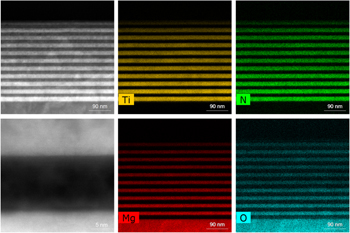
Pulsed laser deposition is one of the most flexible growth methods for high-quality epitaxial multifunctional thin films and short-period superlattices. The following examples of current research interest demonstrate the state-of-the art: First, it is shown that the magnetoelectric performance of multiferroic BiFeO3–BaTiO3 (001)-oriented superlattices depends on the crystalline coherence of the different layers at the interfaces. Second, it is exemplified that dielectric-plasmonic superlattices built from the electrically insulating oxide MgO and the metallically conducting nitride TiN are promising metamaterials with hyperbolic dispersion. As a third example, it is demonstrated that LaNiO3- and LaMnO3-based superlattices with (001)-, (011)-, and (111)-out-of-plane orientation and controlled single layer thickness from 2 to 15 atomic monolayers show metal-insulator transitions and tunable gaps, in partial agreement with density functional theory calculations. Underlined by these examples, it is shown that the precise control of an epitaxially coherent, or two-dimensional layer-by-layer growth, named after Jan van der Merwe, is a prerequisite to achieve the desired functionality of oxide–oxide and oxide–nitride superlattices.

Type
Invited Review
Copyright
Copyright © Materials Research Society 2017 

Access options

Get access to the full version of this content by using one of the access options below. (Log in options will check for institutional or personal access. Content may require purchase if you do not have access.)

Footnotes

Contributing Editor: Mmantsae Diale

This section of Journal of Materials Research is reserved for papers that are reviews of literature in a given area.

References

REFERENCES

Mannhart, J. and Schlom, D.G.: Oxide interfaces—An opportunity for electronics. Science 327, 1607 (2010).Google Scholar
Lorenz, M., Ramachandra Rao, M.S., Venkatesan, T., Fortunato, E., Barquinha, P., Branquinho, R., Salgueiro, D., Martins, R., Carlos, E., Liu, A., Shan, F.K., Grundmann, M., Boschker, H., Mukherjee, J., Priyadarshini, M., DasGupta, N., Rogers, D.J., Teherani, F.H., Sandana, E.V., Bove, P., Rietwyk, K., Zaban, A., Veziridis, A., Weidenkaff, A., Muralidhar, M., Murakami, M., Abel, S., Fompeyrine, J., Zuniga-Perez, J., Ramesh, R., Spaldin, N.A., Ostanin, S., Borisov, V., Mertig, I., Lazenka, V., Srinivasan, G., Prellier, W., Uchida, M., Kawasaki, M., Pentcheva, R., Gegenwart, P., Miletto Granozio, F., Fontcuberta, J., and Pryds, N.: The 2016 oxide electronic materials and oxide interfaces roadmap. J. Phys. D: Appl. Phys. 49, 433001 (2016).Google Scholar
Lorenz, M., Brandt, M., Wagner, G., Hochmuth, H., Zimmermann, G., von Wenckstern, H., and Grundmann, M.: MgZnO:P homoepitaxy by pulsed laser deposition: Pseudomorphic layer-by-layer growth and high electron mobility. Proc. SPIE 7217, 72170N (2009).CrossRefGoogle Scholar
Lorenz, M. and Ramachandra Rao, M.S.: Preface to special issue “25 years of pulsed laser deposition”. J. Phys. D: Appl. Phys. 47, 030301 (2014); see also following articles.Google Scholar
Lorenz, M.: Pulsed laser deposition of ZnO-based thin films, chapter 7. In Transparent Conductive Zinc Oxide. Basics and Applications in Thin Film Solar Cells, Ellmer, K., Klein, A., and Rech, B., eds.; Springer Series in Materials Science, Vol. 104 (Springer, Berlin, 2008); p. 303.Google Scholar
von Wenckstern, H., Schmidt, H., Hanisch, C., Brandt, M., Czekalla, C., Benndorf, G., Biehne, G., Rahm, A., Hochmuth, H., Lorenz, M., and Grundmann, M.: Homoepitaxy of ZnO by pulsed-laser deposition. Phys. Status Solidi RRL 1, 129 (2007).CrossRefGoogle Scholar
Tsukazaki, A., Ohtomo, A., Onuma, T., Ohtani, M., Makino, T., Sumiya, M., Ohtani, K., Chichibu, S.F., Fuke, S., Segawa, Y., Ohno, H., Koinuma, H., and Kawasaki, M.: Repeated temperature modulation epitaxy for p-type doping and light-emitting diode based on ZnO. Nat. Mater. 4, 42 (2005).Google Scholar
Karger, M. and Schilling, M.: Epitaxial properties of Al-doped ZnO thin films grown by pulsed laser deposition on SrTiO3(001). Phys. Rev. B 71, 075304 (2005).Google Scholar
Zippel, J., Lorenz, M., Benndorf, G., and Grundmann, M.: Persistent layer-by-layer growth for pulsed-laser homoepitaxy of (0001) ZnO. Phys. Status Solidi RRL 6, 433 (2012).CrossRefGoogle Scholar
Koster, G., Rijnders, G.J.H.M., Blank, D.H.A., and Rogalla, H.: Imposed layer-by-layer growth by pulsed laser interval deposition. Appl. Phys. Lett. 74, 3729 (1999).CrossRefGoogle Scholar
Lorenz, M., Lazenka, V., Schwinkendorf, P., Bern, F., Ziese, M., Modarresi, H., Volodin, A., Van Bael, M.J., Temst, K., Vantomme, A., and Grundmann, M.: Multiferroic BaTiO3–BiFeO3 composite thin films and multilayers: Strain engineering and magnetoelectric coupling. J. Phys. D: Appl. Phys. 47, 135303 (2014).Google Scholar
Lorenz, M., Wagner, G., Lazenka, V., Schwinkendorf, P., Modarresi, H., Van Bael, M.J., Vantomme, A., Temst, K., Oeckler, O., and Grundmann, M.: Correlation of magnetoelectric coupling in multiferroic BaTiO3–BiFeO3 superlattices with oxygen vacancies and antiphase octahedral rotations. Appl. Phys. Lett. 106, 012905 (2015).Google Scholar
Lorenz, M., Lazenka, V., Schwinkendorf, P., Van Bael, M.J., Vantomme, A., Temst, K., Grundmann, M., and Höche, T.: Epitaxial coherence at interfaces as origin of high magnetoelectric coupling in multiferroic BaTiO3–BiFeO3 superlattices. Adv. Mater. Interfaces 3, 1500822 (2016).Google Scholar
Lazenka, V., Lorenz, M., Modarresi, H., Bisht, M., Rüffer, R., Bonholzer, M., Grundmann, M., Van Bael, M.J., Vantomme, A., and Temst, K.: Magnetic spin structure and magnetoelectric coupling in BiFeO3–BaTiO3 multilayer. Appl. Phys. Lett. 106, 082904 (2015).CrossRefGoogle Scholar
Vaz, C.A.F., Hoffman, J., Ahn, C.H., and Ramesh, R.: Magnetoelectric coupling effects in multiferroic complex oxide composite structures. Adv. Mater. 22, 2900 (2010).CrossRefGoogle ScholarPubMed
Ma, J., Hu, J., Li, Z., and Nan, C-W.: Recent progress in multiferroic magnetoelectric composites: From bulk to thin film. Adv. Mater. 23, 1062 (2011).CrossRefGoogle Scholar
Priya, S., Yang, S.C., Maurya, D., and Yan, Y.: Recent advances in piezoelectric and magnetoelectric materials phenomena. In Composite Magnetoelectrics—Materials, Structures and Applications, Srinivasan, G., Priya, S., and Sun, N.X., eds.; Woodhead Publishing Series in Electronic and Optical Materials No. 62 (Elsevier, Amsterdam, 2015); pp. 103157.Google Scholar
Feng, N., Mi, W., Wang, X., Cheng, Y., and Schwingenschlögl, U.: Superior properties of energetically stable La2/3Sr1/3MnO3/tetragonal BiFeO3 multiferroic superlattices. ACS Appl. Mater. Interfaces 7, 10612 (2015).CrossRefGoogle ScholarPubMed
Gupta, R., Chaudhary, S., and Kotnala, R.K.: Interfacial charge induced magnetoelectric coupling at BiFeO3/BaTiO3 bilayer interface. ACS Appl. Mater. Interfaces 7, 8472 (2015).CrossRefGoogle ScholarPubMed
Kotnala, R.K., Gupta, R., and Chaudhary, S.: Giant magnetoelectric coupling interaction in BaTiO3/BiFeO3/BaTiO3 trilayer multiferroic heterostructures. Appl. Phys. Lett. 107, 082908 (2015).Google Scholar
Popkov, A.F., Davydova, M.D., Zvezdin, K.A., Solov’yov, S.V., and Zvezdin, A.K.: Origin of the giant linear magnetoelectric effect in perovskitelike multiferroic BiFeO3 . Phys. Rev. B 93, 094435 (2016).Google Scholar
Lorenz, M., de Pablos-Martin, A., Patzig, C., Stölzel, M., Brachwitz, K., Hochmuth, H., Grundmann, M., and Höche, T.: Highly textured fresnoite thin films synthesized in situ by pulsed laser deposition with CO2 laser direct heating. J. Phys. D: Appl. Phys. 47, 034013 (2014).Google Scholar
Hansmann, P., Yang, X.P., Toschi, A., Khaliullin, G., Andersen, O.K., and Held, K.: Turning a nickelate Fermi surface into a cupratelike one through heterostructuring. Phys. Rev. Lett. 103, 016401 (2009).CrossRefGoogle ScholarPubMed
Doennig, D., Pickett, W.E., and Pentcheva, R.: Confinement-driven transitions between topological and Mott phases in (LaNiO3) N /(LaAlO3) M (111) superlattices. Phys. Rev. B 89, 121110(R) (2014).Google Scholar
Doennig, D., Baidya, S., Pickett, W.E., and Pentcheva, R.: Design of Chern and Mott insulators in buckled 3d oxide honeycomb lattices. Phys. Rev. B 93, 165145 (2016).Google Scholar
Wei, H.M., Jenderka, M., Bonholzer, M., Grundmann, M., and Lorenz, M.: Modeling the conductivity around the dimensionality-controlled metal-insulator transition in LaNiO3/LaAlO3 (001) superlattices. Appl. Phys. Lett. 106, 042103 (2015).Google Scholar
Wei, H.M., Grundmann, M., and Lorenz, M.: Confinement-driven metal-insulator transition and polarity-controlled conductivity of epitaxial LaNiO3/LaAlO3 (111) superlattices. Appl. Phys. Lett. 109, 082108 (2016).CrossRefGoogle Scholar
Wei, H.M., Barzola-Quiquia, J.L., Yang, C., Patzig, C., Höche, T., Esquinazi, P., Grundmann, M., and Lorenz, M.: Charge transfer-induced magnetic exchange bias and electron localization in (111)- and (001)-oriented LaNiO3/LaMnO3 superlattices. Appl. Phys. Lett. 110, 102403 (2017).Google Scholar
Sass, J., Mazur, K., Surma, B., Eichhorn, F., Litwin, D., Galas, J., and Sitarek, S.: X-ray studies of ultra-thin Si wafers for mirror application. Nucl. Instrum. Methods Phys. Res., Sect. B 253, 236 (2006).Google Scholar
Kawasaki, M., Ohtomo, A., Arakane, T., Takahashi, K., Yoshimoto, M., and Koinuma, H.: Atomic control of SrTiO3 surface for perfect epitaxy of perovskite oxides. Appl. Surf. Sci. 107, 102 (1996).Google Scholar
Koster, G., Rijnders, G., Blank, D.H.A., and Rogalla, H.: Surface morphology determined by (001) single-crystal SrTiO3 termination. Physica C 339, 215 (2000).Google Scholar
Wei, H.M.: Conductivity behavior of LaNiO3- and LaMnO3-based thin film superlattices. Ph.D. thesis, Universität Leipzig, Fakultät für Physik und Geowissenschaften, Leipzig, Germany, 2017.Google Scholar
Bonholzer, M., Lorenz, M., and Grundmann, M.: TiN layer-by-layer growth of TiN by pulsed laser deposition on in situ annealed (100) MgO substrates. Phys. Status Solidi A 211, 2621 (2014).CrossRefGoogle Scholar
Lorenz, M., Hochmuth, H., Grüner, C., Hilmer, H., Lajn, A., Spemann, D., Brandt, M., Zippel, J., Schmidt-Grund, R., von Wenckstern, H., and Grundmann, M.: Oxide thin film heterostructures on large area, with flexible doping, low dislocation density, and abrupt interfaces: Grown by pulsed laser deposition. Laser Chem. 2010, 140976 (2010).Google Scholar
Höche, Th., Gerlach, J.W., and Petsch, T.: Static-charging mitigation and contamination avoidance by selective carbon coating of TEM samples. Ultramicroscopy 106, 981 (2006).CrossRefGoogle ScholarPubMed
Lorenz, M., Hirsch, D., Patzig, C., Höche, T., Hohenberger, S., Hochmuth, H., Lazenka, V., Temst, K., and Grundmann, M.: Correlation of interface impurities and chemical gradients with high magnetoelectric coupling strength in multiferroic BiFeO3–BaTiO3 superlattices. ACS Appl. Mater. Interfaces 9, 1895618965 (2017).CrossRefGoogle Scholar
Naik, G.V., Schroeder, J.L., Ni, X., Kildishev, A.V., Sands, T.D., and Boltasseva, A.: Titanium nitride as a plasmonic material for visible and near-infrared wavelengths. Opt. Mater. Express 2, 478 (2012).Google Scholar
Salandrino, A. and Engheta, N.: Far-field subdiffraction optical microscopy using metamaterial crystals: Theory and simulations. Phys. Rev. B 74, 075103 (2006).CrossRefGoogle Scholar
Naik, G.V., Saha, B., Liu, J., Saber, S.M., Stach, E.A., Irudayaraj, J.M.K., Sands, T.D., Shalaev, V.M., and Boltasseva, A.: Epitaxial superlattices with titanium nitride as a plasmonic component for optical hyperbolic metamaterials. Proc. Natl. Acad. Sci. U. S. A. 111, 7546 (2014).Google Scholar
Boris, A.V., Matiks, Y., Benckiser, E., Frano, A., Popovich, P., Hinkov, V., Wochner, P., Colin, M.C., Detemple, E., Malik, V.K., Bernhard, C., Prokscha, T., Suter, A., Salman, Z., Morenzoni, E., Cristiani, G., Habermeier, H.U., and Keimer, B.: Dimensionality control of electronic phase transitions in nickel–oxide superlattices. Science 332, 937 (2011).Google Scholar
Gibert, M., Zubko, P., Scherwitzl, R., Íñiguez, J., and Triscone, J-M.: Exchange bias in LaNiO3–LaMnO3 superlattices. Nat. Mater. 11, 195 (2012).Google Scholar