Hostname: page-component-745bb68f8f-b95js Total loading time: 0 Render date: 2025-01-11T00:27:53.793Z Has data issue: false hasContentIssue false

Titanium dioxide thin films for next-generation memory devices

Published online by Cambridge University Press:  19 July 2012

Seong Keun Kim
Affiliation:
Electronic Materials Research Center, Korea Institute of Science and Technology, Seoul 130-650, Korea
Kyung Min Kim
Affiliation:
Semiconductor Laboratory, Samsung Advanced Institute of Technology, Gyeonggi-Do 446-712, Korea
Doo Seok Jeong
Affiliation:
Electronic Materials Research Center, Korea Institute of Science and Technology, Seoul 130-650, Korea
Woojin Jeon
Affiliation:
Department of Materials Science and Engineering, WCU Hybrid Materials Program, Seoul National University, Seoul 151-744, Korea; and Inter-university Semiconductor Research Center, Seoul National University, Seoul 151-744, Korea
Kyung Jean Yoon
Affiliation:
Department of Materials Science and Engineering, WCU Hybrid Materials Program, Seoul National University, Seoul 151-744, Korea; and Inter-university Semiconductor Research Center, Seoul National University, Seoul 151-744, Korea
Cheol Seong Hwang*
Affiliation:
Department of Materials Science and Engineering, WCU Hybrid Materials Program, Seoul National University, Seoul 151-744, Korea; and Inter-university Semiconductor Research Center, Seoul National University, Seoul 151-744, Korea
*
a)Address all correspondence to this author. e-mail: [email protected]
Get access

Abstract

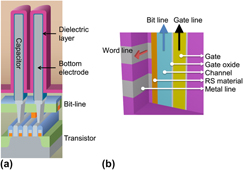
The synthesis, structure, and electrical performances of titanium dioxide (TiO2 and also doped TiO2) thin films, a capacitor dielectric for dynamic random access memory (DRAM) and a resistance switching material in resistance switching RAM (ReRAM), are reviewed. The three-dimensionality of these structures and the extremely small feature sizes (<20 nm) of these memory devices require the synthesis method of TiO2-based layers to exhibit high degree of conformality. Atomic layer deposition is, therefore, the method of choice in respect of film growth for these applications. The unique arrangement of the TiO6-octahedra in the rutile structure, which results in the value for dielectric constant of the dielectric layer, εr (>100), makes the material especially attractive as the capacitor dielectric layer in DRAM. Removing some of the oxygen ions from the rutile structure and arranging the resulting oxygen vacancies on a specific crystallographic plane results in the so called Magnéli phase materials, which show distinctive conducting semiconductor or metallic characteristics. External electrical stimuli can cause the repeated formation and rupture of conducting channels that consist of these Magnéli phase materials in the insulating TiO2 matrix, and this aspect makes the material a very feasible choice for applications in ReRAM. This article reviews the material properties, fabrication process, integration issues, and prospect of TiO2 films for these applications.

Type
Reviews
Copyright
Copyright © Materials Research Society 2012

Access options

Get access to the full version of this content by using one of the access options below. (Log in options will check for institutional or personal access. Content may require purchase if you do not have access.)

References

REFERENCES

Tanaka, H., Kido, M., Yahashi, K., Oomura, M., Katsumata, R., Kito, M., Fukuzumi, Y., Sato, M., Nagata, Y., Matsuoka, Y., Iwata, Y., Aochi, H., and Nitayama, A.: Bit-cost scalable technology with punch and plug process for ultrahigh density flash memory. VLSI Symp. Tech. Dig. 14 (2007).Google Scholar
Wilk, G.D., Wallace, R.M., and Anthony, J.M.: High-κ gate dielectrics: Current status and materials properties considerations. J. Appl. Phys. 89, 5243 (2001).CrossRefGoogle Scholar
Sawa, A.: Resistive switching in transition metal oxides. Mater. Today 11(6), 28 (2008).CrossRefGoogle Scholar
Waser, R., Dittmann, R., Staikov, G., and Szot, K.: Redox-based resistive switching memories—Nanoionic mechanisms, prospects, and challenges. Adv. Mater. 21, 2632 (2009).CrossRefGoogle ScholarPubMed
Choi, B.J., Jeong, D.S., Kim, S.K., Rohde, C., Choi, S., Oh, J.H., Kim, H.J., Hwang, C.S., Szot, K., Waser, R., Reichenberg, B., and Tiedke, S.: Resistive switching mechanism of TiO2 thin films grown by atomic layer deposition. J. Appl. Phys. 98, 033715 (2005).CrossRefGoogle Scholar
Fujimoto, M., Koyama, H., Konagai, M., Hosoi, Y., Ishihara, K., Ohnishi, S., and Awaya, N.: TiO2 anatase nanolayer on TiN thin film exhibiting high-speed bipolar resistive switching. Appl. Phys. Lett. 89, 223509 (2006).CrossRefGoogle Scholar
Tsunoda, K., Fukuzumi, Y., Jameson, J.R., Wang, Z., Griffin, P.B., and Nishi, Y.: Bipolar resistive switching in polycrystalline TiO2 films. Appl. Phys. Lett. 90, 113501 (2007).CrossRefGoogle Scholar
Lee, M-J., Seo, S., Kim, D-C., Ahn, S-E., Seo, D.H., Yoo, I-K., Baek, I-G., Kim, D-S., Byun, I-S., Kim, S-H., Hwang, I-R., Kim, J-S., Jeon, S-H., and Park, B.H.: A low-temperature-grown oxide diode as a new switch element for high-density, nonvolatile memories. Adv. Mater. 19, 73 (2007).CrossRefGoogle Scholar
Baek, I.G., Park, C.J., Ju, H., Seong, D.J., Ahn, H.S., Kim, J.H., Yang, M.K., Song, S.H., Kim, E.M., Park, S.O., Park, C.H., Song, C.W., Jeong, G.T., Choi, S., Kang, H.K., and Chung, C.: Realization of vertical resistive memory (VRRAM) using cost effective 3D process. IEEE Int. Electron Devices Meeting 31.8.1 (2011).Google Scholar
Yang, J.J., Strachan, J.P., Miao, F., Zhang, M-X., Pickett, M.D., Yi, W., Ohlberg, D.A.A., Medeiros-Ribeiro, G., and Williams, R.S.: Metal/TiO2 interfaces for memristive switches. Appl. Phys. A 102, 785 (2011).CrossRefGoogle Scholar
Kofstad, P.: Thermogravimetric studies of the defect structure of rutile (TiO2). J. Phys. Chem. Solids 23, 1579 (1962).CrossRefGoogle Scholar
Balachandran, U. and Eror, N.G.: Electrical conductivity in nonstoichiometric titanium dioxide at elevated temperatures. J. Mater. Sci. 23, 2676 (1988).CrossRefGoogle Scholar
Marucco, J-F., Gautron, J., and Lemasson, P.: Thermogravimetric and electrical study of nonstoichiometric titanium dioxide TiO2-x, between 800 and 1100 C. J. Phys. Chem. Solids 42, 363 (1981).CrossRefGoogle Scholar
Meis, C. and Fleche, J.L.: Study of the solubility limit of oxygen vacancies in TiO2-x using molecular dynamics. Solid State Ionics 101103(Part 1), 333 (1997).Google Scholar
Baumard, J.F., Panis, D., and Anthony, A.M.: A study of Ti-O system between Ti3O5 and TiO2 at high temperature by means of electrical resistivity. J. Solid State Chem. 20, 43 (1977).CrossRefGoogle Scholar
Hasiguti, R.R.: The structure of defects in solids. Ann. Rev. Mater. Sci. 2, 69 (1972).CrossRefGoogle Scholar
Andersson, P.O., Kollberg, E.L., and Jelenski, A.: Charge compensation in iron-doped rutile. J. Phys. C: Solid State Phys. 7, 1868 (1974).CrossRefGoogle Scholar
Banus, M.D. and Reed, T.B.: The Chemistry of Extended Defects in Nonmetallic Solids (North-Holland, Amsterdam, 1970).Google Scholar
Bursill, L.A. and Hyde, B.G.: Crystallographic shear in the higher titanium oxides: Structure, texture, mechanisms and thermodynamics. Prog. Solid State Chem. 7, 177 (1972).CrossRefGoogle Scholar
Jeong, D.S., Schroeder, H., and Waser, R.: Mechanism for bipolar switching in a Pt/TiO2/Pt resistive switching cell. Phys. Rev. B 79, 195317 (2009).CrossRefGoogle Scholar
Kim, G.H., Lee, J.H., Seok, J.Y., Song, S.J., Yoon, J.H., Yoon, K.J., Lee, M.H., Kim, K.M., Lee, H.D., Ryu, S.W., Park, T.J., and Hwang, C.S.: Improved endurance of resistive switching TiO2 thin film by hourglass-shaped Magnéli filaments. Appl. Phys. Lett. 98, 262901 (2011).Google Scholar
Kwon, D-H., Kim, K.M., Jang, J.H., Jeon, J.M., Lee, M.H., Kim, G.H., Li, X-S., Park, G-S., Lee, B., Han, S., Kim, M., and Hwang, C.S.: Atomic structure of conducting nanofilaments in TiO2 resistive switching memory. Nat. Nanotechnol. 5, 148 (2010).CrossRefGoogle ScholarPubMed
Strachan, J.P., Pickett, M.D., Yang, J.J., Aloni, S., David Kilcoyne, A.L., Medeiros-Ribeiro, G., and Williams, R.S.: Direct identification of the conducting channels in a functioning memristive device. Adv. Mater. 22, 3573 (2010).CrossRefGoogle Scholar
Kim, S.K., Lee, S.W., Han, J.H., Lee, B., Han, S., and Hwang, C.S.: Capacitors with an equivalent oxide thickness of <0.5 nm for nanoscale electronic semiconductor memory. Adv. Funct. Mater. 20, 2989 (2010).CrossRefGoogle Scholar
Seok, J.Y., Kim, G.H., Kim, J.H., Kim, U.K., Chung, Y.J., Song, S.J., Yoon, J.H., Yoon, K.J., Lee, M.H., Kim, K.M., and Hwang, C.S.: Resistive switching in TiO2 thin films using the semiconducting In-Ga-Zn-O electrode. IEEE Electron Device Lett. 33, 582 (2012).CrossRefGoogle Scholar
Leskelä, M. and Ritala, M.: Atomic layer deposition chemistry: Recent developments and future challenges. Angew. Chem. Int. Ed. 42, 5548 (2003).CrossRefGoogle ScholarPubMed
Suntola, T.: Atomic layer epitaxy. Mater. Sci. Rep. 4, 261 (1989).CrossRefGoogle Scholar
Leskelä, M. and Ritala, M.: Atomic layer deposition (ALD): From precursors to thin film structures. Thin Solid Films 409, 138 (2002).CrossRefGoogle Scholar
Kuesters, K.H., Beug, M.F., Schroeder, U., Nagel, N., Bewersdorff, U., Dallmann, G., Jakschik, S., Knoefler, R., Kudelka, S., Ludwig, C., Manger, D., Mueller, W., and Tilke, A.: New materials in memory development sub 50 nm: Trends in Flash and DRAM. Adv. Eng. Mater. 11, 241 (2009).CrossRefGoogle Scholar
Gordon, R.G., Hausmann, D., Kim, E., and Shepard, J.: A kinetic model for step coverage by atomic layer deposition in narrow holes or trenches. Chem. Vap. Deposition 9, 73 (2003).CrossRefGoogle Scholar
Kim, S.K., Kim, K-M., Kwon, O.S., Lee, S.W., Jeon, C.B., Park, W.Y., Hwang, C.S., and Jeong, J.: Structurally and electrically uniform deposition of high-k TiO2 thin films on a Ru electrode in three-dimensional contact holes using atomic layer deposition. Electrochem. Solid-State Lett. 8(12), F59 (2005).CrossRefGoogle Scholar
Kim, W.D., Hwang, G.W., Kwon, O.S., Kim, S.K., Cho, M., Jeong, D.S., Lee, S.W., Seo, M.H., Hwang, C.S., Min, Y-S., and Cho, Y.J.: Growth characteristics of atomic layer deposited TiO2 thin films on Ru and Si electrodes for memory capacitor applications. J. Electrochem. Soc. 152(8), C552 (2005).CrossRefGoogle Scholar
Kim, S.K., Hoffmann-Eifert, S., and Waser, R.: High growth rate in atomic layer deposition of TiO2 thin films by UV irradiation. Electrochem. Solid-State Lett. 14(4), H146 (2011).CrossRefGoogle Scholar
Kim, S.K., Hoffmann-Eifert, S., Mi, S., and Waser, R.: Liquid injection atomic layer deposition of crystalline TiO2 thin films with a smooth morphology from Ti(O-i-Pr)2(DPM)2. J. Electrochem. Soc. 156(8), D296 (2009).CrossRefGoogle Scholar
Aarik, J., Aidla, A., Mändar, H., and Uustare, T.: Atomic layer deposition of titanium dioxide from TiCl4 and H2O: Investigation of growth mechanism. Appl. Surf. Sci. 172, 148 (2001).CrossRefGoogle Scholar
Diebold, U.: The surface science of titanium dioxide. Surf. Sci. Rep. 48, 53 (2003).CrossRefGoogle Scholar
Lee, C., Ghosez, P., and Gonze, X.: Lattice-dynamics and dielectric properties of incipient ferroelectric TiO2 rutile. Phys. Rev. B 50, 13379 (1994).CrossRefGoogle ScholarPubMed
Aarik, J., Aidla, A., Uustare, T., Kukli, K., Sammelselg, V., Ritala, M., and Leskelä, M.;: Atomic layer deposition of TiO2 thin films from TiI4 and H2O. Appl. Surf. Sci. 193, 277 (2002).CrossRefGoogle Scholar
Schuisky, M., Aarik, J., Kukli, K., Aidla, A., and Hårsta, A.: Atomic layer deposition of thin films using O2 as oxygen source. Langmuir 17, 5508 (2001).CrossRefGoogle Scholar
Kim, S.K., Kim, W-D., Kim, K-M., Hwang, C.S., and Jeong, J.: High dielectric constant TiO2 thin films on a Ru electrode grown at 250 °C by atomic layer deposition. Appl. Phys. Lett. 85(18), 4112 (2004).CrossRefGoogle Scholar
Kim, S.K., Hwang, G.W., Kim, W-D., and Hwang, C.S.: Transformation of the crystalline structure of an ALD TiO2 film on a Ru electrode by O3 pretreatment. Electrochem. Solid-State Lett. 9(1), F5 (2006).CrossRefGoogle Scholar
Kim, S.K., Lee, S.Y., Seo, M., Choi, G-J., and Hwang, C.S.: Impact of O3 feeding time on TiO2 films grown by atomic layer deposition for memory capacitor applications. J. Appl. Phys. 102, 024109 (2007).CrossRefGoogle Scholar
Green, M.L., Gross, M.E., Papa, L.E., Schnoes, K.L., and Brasen, D.: Chemical vapor deposition of ruthenium and ruthenium dioxide films. J. Electrochem. Soc. 132, 2677 (1985).CrossRefGoogle Scholar
Han, J.H., Han, S., Lee, W., Lee, S.W., Kim, S.K., Gatineau, J., Dussarrat, C., and Hwang, C.S.: Improvement in the leakage current characteristic of metal-insulator-metal capacitor by adopting RuO2 film as bottom electrode. Appl. Phys. Lett. 99, 022901 (2011).CrossRefGoogle Scholar
Fröhlich, K., Aarik, J., Ťapajna, M., Rosová, A., Aidla, A., Dobročka, E., and Hušková, K.: Epitaxial growth of high-kappa TiO2 rutile films on RuO2 electrodes. J. Vac. Sci. Technol., B 27, 266 (2009).CrossRefGoogle Scholar
Kim, S.K., Han, S., Han, J.H., Lee, W., and Hwang, C.S.: Atomic layer deposition of TiO2 and Al-doped TiO2 films on Ir substrates for ultralow leakage currents. Phys. Status Solidi RRL 5, 262 (2011).CrossRefGoogle Scholar
Kim, S.K., Choi, G-J., Lee, S.Y., Seo, M., Lee, S.W., Han, J.H., Ahn, H-S., Han, S., and Hwang, C.S.: Al-doped TiO2 films with ultralow leakage currents for next generation DRAM capacitors. Adv. Mater. 20, 1429 (2008).CrossRefGoogle Scholar
Seo, M., Kim, S.K., Han, J.H., and Hwang, C.S.: Permittivity enhanced atomic layer deposited HfO2 thin films manipulated by a rutile TiO2 interlayer. Chem. Mater. 22, 4419 (2010).CrossRefGoogle Scholar
Seo, M., Rha, S-H., Kim, S.K., Han, J.H., Lee, W., Han, S., and Hwang, C.S.: The mechanism for the suppression of leakage current in high dielectric TiO2 thin films by adopting ultrathin HfO2 films for memory application. J. Appl. Phys. 110, 024105 (2011).CrossRefGoogle Scholar
Hwang, C.S.: Thickness-dependent dielectric constants of (Ba, Sr)TiO3 thin films with Pt or conducting oxide electrodes. J. Appl. Phys. 92, 432 (2002).CrossRefGoogle Scholar
Black, C.T. and Welser, J.J.: Electric-field penetration into metals: Consequences for high-dielectric-constant capacitors. IEEE Trans. Electron Devices 46, 776 (1999).CrossRefGoogle Scholar
Stengel, M. and Spaldin, N.A.: Origin of the dielectric dead layer in nanoscale capacitors. Nature 443, 679 (2006).CrossRefGoogle ScholarPubMed
Jeong, D.S., Schroeder, H., and Waser, R.: Coexistence of bipolar and unipolar resistive switching behaviors in a Pt/TiO2/Pt stack. Electrochem. Solid-State Lett. 10(8), G51 (2007).CrossRefGoogle Scholar
Kim, K.M., Choi, B.J., Lee, M.H., Kim, G.H., Song, S.J., Seok, J.Y., Yoon, J.H., Han, S. and Hwang, C.S.: A detailed understanding of the electronic bipolar resistance switching behavior in Pt/TiO2/Pt structure. Nanotechnology 22, 254010 (2011).CrossRefGoogle ScholarPubMed
Rohde, C., Choi, B.J., Jeong, D.S., Choi, S., Zhao, J-S., and Hwang, C.S.: Identification of a determining parameter for resistive switching of TiO2 thin films. Appl. Phys. Lett. 86, 262907 (2005).CrossRefGoogle Scholar
Shin, Y.C., Lee, M.H., Kim, K.M., Kim, G.H., Song, S.J., Seok, J.Y., and Hwang, C.S.: Bias polarity dependent local electrical conduction in resistive switching TiO2 thin films. Phys. Status Solidi RRL 4(5–6), 112 (2010).CrossRefGoogle Scholar
Kim, K.M. and Hwang, C.S.: The conical shape filament growth model in unipolar resistance switching of TiO2 thin film. Appl. Phys. Lett. 94, 122109 (2009).CrossRefGoogle Scholar
Kim, K.M., Choi, B.J., Shin, Y.C., Choi, S., and Hwang, C.S.: Anode-interface localized filamentary mechanism in resistive switching of TiO2 thin films. Appl. Phys. Lett. 91, 012907 (2007).CrossRefGoogle Scholar
Kim, K.M., Choi, B.J., and Hwang, C.S.: Localized switching mechanism in resistive switching of atomic-layer-deposited TiO2 thin films. Appl. Phys. Lett. 90, 242906 (2007).CrossRefGoogle Scholar
Kim, K.M., Jeong, D.S., and Hwang, C.S.: Nanofilamentary resistive switching in binary oxide system: A review on the present status and outlook. Nanotechnology 22, 254002 (2011).CrossRefGoogle ScholarPubMed
Kim, K.M., Kim, G.H., Song, S.J., Seok, J.Y., Lee, M.H., Yoon, J.H., and Hwang, C.S.: Electrically configurable electroforming and bipolar resistive switching in Pt/TiO2/Pt structures. Nanotechnology 21, 305203 (2010).CrossRefGoogle ScholarPubMed
Yoon, K.J., Lee, M.H., Kim, G.H., Song, S.J., Seok, J.Y., Han, S.R., Yoon, J.H., Kim, K.M., and Hwang, C.S.: Memristive tristable resistive switching at ruptured conducting filaments of a Pt/TiO2/Pt cell. Nanotechnology 23, 185202 (2012).CrossRefGoogle Scholar
Yang, J.J., Pickett, M.D., Li, X., Ohlberg, D.A.A., Stewart, D.R., and Williams, R.S.: Memristive switching mechanism for metal/oxide/metal nanodevices. Nat. Nanotechnol. 3, 429 (2008).CrossRefGoogle ScholarPubMed