Hostname: page-component-586b7cd67f-2plfb Total loading time: 0 Render date: 2024-11-26T22:04:28.388Z Has data issue: false hasContentIssue false

Study of phase separation in an InGaN alloy by electron energy loss spectroscopy in an aberration corrected monochromated scanning transmission electron microscope

Published online by Cambridge University Press:  08 December 2016

Thomas Walther*
Affiliation:
Department Electronic & Electrical Eng., Kroto Centre for High-Resolution Imaging and Spectroscopy, University of Sheffield, Sheffield S3 7HQ, U.K.
Xiaoyi Wang
Affiliation:
Department Electronic & Electrical Eng., Kroto Centre for High-Resolution Imaging and Spectroscopy, University of Sheffield, Sheffield S3 7HQ, U.K.
Veerendra C. Angadi
Affiliation:
Department Electronic & Electrical Eng., Kroto Centre for High-Resolution Imaging and Spectroscopy, University of Sheffield, Sheffield S3 7HQ, U.K.
Pierre Ruterana
Affiliation:
CIMAP, UMR 6252, CNRS-ENSICAEN-CEA-UCBN, 14050 Caen, Cedex, France
Paolo Longo
Affiliation:
Gatan, Warrendale, PA15086, USA
Toshihiro Aoki
Affiliation:
LeRoy Eyring Center for Solid State Science, Arizona State University, Tempe, AZ85287, USA
*
a)Address all correspondence to this author. e-mail: [email protected]
Get access

Abstract

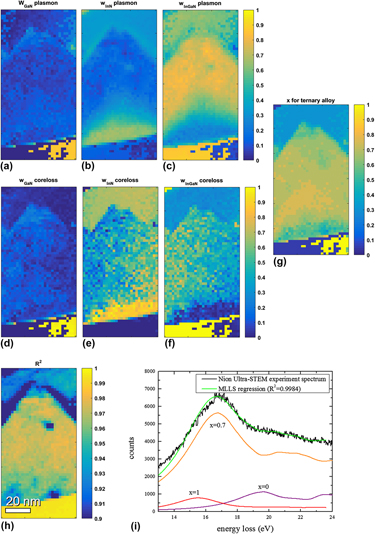
Phase separation of InxGa1−xN into Ga-rich and In-rich regions has been studied by electron energy-loss spectroscopy (EELS) in a monochromated, aberration corrected scanning transmission electron microscope (STEM). We analyze the full spectral information contained in EELS of InGaN, combining for the first time studies of high-energy and low-energy ionization edges, plasmon, and valence losses. Elemental maps of the N K, In M4,5 and Ga L2,3 edges recorded by spectrum imaging at 100 kV reveal sub-nm fluctuations of the local indium content. The low energetic edges of Ga M4,5 and In N4,5 partially overlap with the plasmon peaks. Both have been fitted iteratively to a linear superimposition of reference spectra for GaN, InN, and InGaN, providing a direct measurement of phase separation at the nm-scale. Bandgap measurements are limited in real space by scattering delocalization rather than the electron beam size to ∼10 nm for small bandgaps, and their energetic accuracy by the method of fitting the onset of the joint density of states rather than energy resolution. For an In0.62Ga0.38N thin film we show that phase separation occurs on several length scales.

Type
Articles
Copyright
Copyright © Materials Research Society 2016 

Access options

Get access to the full version of this content by using one of the access options below. (Log in options will check for institutional or personal access. Content may require purchase if you do not have access.)

Footnotes

Contributing Editor: Eric A. Stach

b)

This author was an editor of this journal during the review and decision stage. For the JMR policy on review and publication of manuscripts authored by editors, please refer to http://www.mrs.org/editor-manuscripts/.

A previous error in this article has been corrected, see 10.1557/jmr.2017.245.

References

REFERENCES

Ruterana, P., Nouet, G., Van der Stricht, W., Moerman, I., and Considine, L.: Chemical ordering in wurtzite In x Ga1−x N layers grown on (0001) sapphire by metalorganic vapor phase epitaxy. Appl. Phys. Lett. 72(14), 1742 (1998).CrossRefGoogle Scholar
Zhu, D.M., You, S., Detchprohm, T., Paskova, T., Preble, E.A., Hanser, D., and Wetzel, C.: Inclined dislocation-pair relaxation mechanism in homoepitaxial green GaInN/GaN light-emitting diodes. Phys. Rev. B: Condens. Matter Mater. Phys. 81(12), 125325 (2010).Google Scholar
Doppalapudi, D., Basu, S.N., Ludwig, K.F. Jr., and Moustakas, T.D.: Phase separation and ordering in InGaN alloys grown by molecular beam epitaxy. J. Appl. Phys. 84(3), 1389 (1998).Google Scholar
Park, I-K., Kwon, M.K., Baek, S-H., Ok, Y-W., Seong, T-Y., Park, S-J., Kim, Y-S., Moon, Y-T., and Kim, D-J.: Enhancement of phase separation in the InGaN layer for self-assembled In-rich quantum dots. Appl. Phys. Lett. 87, 061906 (2005).Google Scholar
Lin, Y-S., Ma, K-J., Hsu, C., Feng, S-W., Cheng, Y-C., Liao, C-C., Yang, C-C., Chou, C-C., Lee, C-M., and Chyi, J.I.: Dependence of composition fluctuation on indium content in InGaN/GaN multiple quantum wells. Appl. Phys. Lett. 77(19), 2988 (2000).Google Scholar
Singh, R., Doppalapudi, D., Moustakas, T.D., and Romano, L.T.: Phase separation in InGaN thick films and formation of InGaN/GaN double heterostructures in the entire alloy composition. Appl. Phys. Lett. 70, 1089 (1997).Google Scholar
Ho, I.H. and Stringfellow, G.B.: Solid phase immiscibility in GaInN. Appl. Phys. Lett. 69(18), 2701 (1996).Google Scholar
Matsuoka, T., Sasaki, T., and Katsui, A.: Growth and properties of a wide-gap semiconductor indium gallium nitride. Optoelectron. Devices Technol. 5(1), 53 (1990).Google Scholar
Matsuoka, T., Yoshimoto, N., Sasaki, T., and Katsui, A.: Wide-gap semiconductor InGaN and InGaAlN grown by MOVPE. J. Electron. Mater. 21(2), 157 (1992).Google Scholar
Nakamura, S.: Growth of In x Ga1−x N compound semiconductors and high-power InGaN/AlGaN double-heterostructure violet-light-emitting diodes. Microelectron. J. 25(8), 651 (1994).Google Scholar
Shimizu, M., Hiramatsu, K., and Sawaki, N.: Metalorganic vapor-phase epitaxy growth of (In x Ga1−x N/GaN) layered structures and reduction of indium droplets. J. Cryst. Growth. 145, 209 (1994).CrossRefGoogle Scholar
Nakamura, S., Mukai, T., Senoh, M., Nagahama, S., and Iwasa, N.: In x Ga1−x N/In y Ga1−y N superlattices grown on GaN films. J. Appl. Phys. 74(6), 3911 (1993).Google Scholar
O’Neill, J.P., Ross, I.M., Cullis, A.G., Wang, T., and Parbrook, P.J.: Electron-beam-induced segregation in InGaN/GaN multiple-quantum wells. Appl. Phys. Lett. 83(10), 1965 (2003).Google Scholar
Smeeton, T.M., Kappers, M.J., Barnard, J.S., Vickers, M.E., and Humphreys, C.J.: Electron-beam-induced strain within InGaN quantum wells: False indium “cluster” detection in the transmission electron microscope. Appl. Phys. Lett. 83(26), 5419 (2003).Google Scholar
Humphreys, C.J.: Does In form In-rich clusters in InGaN quantum wells? Philos. Mag. 87(13), 1971 (2007).Google Scholar
Baloch, K.H., Johnston-Peck, A.C., Kisslinger, K., Stach, E.A., and Gradecak, S.: Revisiting the “In-clustering” question in InGaN through the use of aberration corrected electron microscopy below the knock-on threshold. Appl. Phys. Lett. 102, 191910 (2013).Google Scholar
Wang, X., Chauvat, M-P., Ruterana, P., and Walther, T.: Investigation of phase separation in InGaN alloys by plasmon loss spectroscopy in a TEM. MRS Adv. 1(40), 27492756 (2016). doi: 10.1557/adv2016.542.Google Scholar
Wang, X., Chauvat, M.P., Ruterana, P., and Walther, T.: Combination of electron energy-loss spectroscopy and energy-dispersive x-ray spectroscopy to determine indium concentration in InGaN thin film structures. Semicond. Sci. Technol. 30(11), 114011 (2015).Google Scholar
Walther, T., Wolf, F., Recnik, A., and Mader, W.: Quantitative microstructural and spectroscopic investigation of inversion domain boundaries in zinc oxide ceramics sintered with iron oxide. Int. J. Mater. Res. 97, 934 (2006).Google Scholar
Krivanek, O.L., Ursin, J.P., Bacon, N.J., Corbin, G.J., Dellby, N., Hrncirik, P., Murfitt, M.F., Own, C.S., and Szylagyi, Z.S.: High-energy-resolution monochromator for aberration-corrected scanning transmission electron microscope/electron energy-loss spectroscopy. Phil. Trans. R. Soc., A 367(1903), 3683 (2009).Google Scholar
Bartel, T.P., Specht, P., Ho, J.C., and Kisielowski, C.: Phase separation in In x Ga1−x N. Philos. Mag. 87(13), 1983 (2007).Google Scholar
Orsal, G., El Gmili, Y., Fressengeas, N., Streque, J., Djerboub, R., Moudakir, T., Sundaram, D., Ougazzaden, A., and Salvestrini, J.P.: Bandgap energy bowing parameter of strained and relaxed InGaN layers. Opt. Mater. Express 4(5), 1030 (2014).CrossRefGoogle Scholar
Walther, T.: An improved approach to quantitative x-ray microanalysis in (S)TEM: Thickness dependent k-factors. Proc EMAG 2009, Sheffield. J. Phys. Conf. Ser. 241, 012016 (2010).Google Scholar
Walther, T. and Wang, X.: Self-consistent method for quantifying indium content from x-ray spectra of thick compound semiconductor specimens in a transmission electron microscope. J. Microsc. 252(2), 151 (2016).Google Scholar
Amari, H., Ross, I.M., Wang, T., and Walther, T.: Characterization of InGaN/GaN epitaxial layers by aberration corrected TEM/STEM. Phys. Stat. Sol. C 9(3–4), 546 (2012).Google Scholar
Egerton, R.F.: Electron Energy-loss Spectroscopy in the Electron Microscope, 2nd ed. (Plenum Press, New York, 1996).CrossRefGoogle Scholar
Angadi, V.C., Abhayaratne, C., and Walther, T.: Automated background subtraction technique for electron energy-loss spectroscopy and application to semiconductor heterostructures. J. Microsc. 262(2), 157 (2016).Google Scholar
Thomas, P.J. and Twesten, R.D.: A simple, model based approach for robust quantification of EELS spectra and spectrum-images. Microsc. Microanal. 18(Suppl. 2), 968 (2012).CrossRefGoogle Scholar
Scott, J., Thomas, P.J., MacKenzie, M., McFadzean, S., Wilbrink, J., Craven, A.J., and Nicholson, W.A.P.: Near-simultaneous dual energy range EELS spectrum imaging. Ultramicrosocpy 108(12), 1586 (2008).Google Scholar
Jinschek, J.R., Erni, R., Gardner, N.F., Kim, A.Y., and Kisielowski, C.: Local indium segregation and band gap variations in high efficiency green light emitting InGaN/GaN diodes. Solid State Comm. 137, 230 (2006).CrossRefGoogle Scholar
Albrecht, M., Grillo, V., Borysiuk, J., Remmele, T., Strunk, H.P., Walther, T., Mader, W., Prystawko, P., Leszczynski, M., Grzegory, I., and Porowski, S.: Correlating compositional, structural and optical properties of InGaN quantum wells by transmission electron microscopy. Proc. Microsc. Semicond. Mater. Conf. 2001, Oxford. Inst. Phys. Conf. Ser. 169, 267 (2001).Google Scholar
Erni, R. and Browning, N.D.: Valence electron energy-loss spectroscopy in monochromated scanning transmission electron microscopy. Ultramicroscopy 104(3–4), 176 (2005).Google Scholar
Walther, T. and Stegmann, H.: Preliminary results from the first monochromated and aberration corrected 200-kV field-emission scanning transmission electron microscope. Microsc. & Microanal. 12(6), 498 (2006).Google Scholar
Brockt, G. and Lakner, H.: Nanoscale EELS analysis of dielectric function and bandgap properties in GaN and related materials. Micron 31, 435 (2000).Google Scholar
Schamm, S. and Zanchi, G.: Study of the dielectric properties near the band gap by VEELS: Gap measurement in bulk materials. Ultramicroscopy 96, 559 (2003).Google Scholar
Manual, J.M., Koch, C.T., Özdöl, V.B., Sigle, W., van Aken, P.A., Garcia, R., and Morales, F.M.: Inline electron holography and VEELS for the measurement of strain in ternary and quaternary (In,Al,Ga)N alloyed thin films and its effect on bandgap energy. J. Microsc. 261(1), 27 (2016).Google Scholar
Stöger-Pollach, M. and Schattschneider, P.: The influence of relativistic energy losses on bandgap determination using valence EELS. Ultramicroscopy 107(12), 1178 (2007).Google Scholar
Müllejans, H. and French, R.H.: Insights into the electronic structure of ceramics through quantitative analysis of valence energy-loss spectroscopy. Microsc. Microanal. 6(4), 297 (2000).CrossRefGoogle ScholarPubMed
Specht, P., Ho, J.C., Xu, X., Armitage, R., Weber, E.R., Erni, R., and Kisielowski, C.: Band transitions in wurtzite GaN and InN determined by valence electron energy loss spectroscopy. Sol. State Comm. 135, 340 (2005).Google Scholar
Erni, R. and Browning, N.D.: Quantification of the size-dependent energy gap of individual CdSe quantum dots by valence electron energy-loss spectroscopy. Ultramicroscopy 107(2–3), 267 (2007).Google Scholar
Pelá, R.R., Caetano, C., Marques, M., Ferreira, L.G., Furthmüller, J., and Teles, L.K.: Accurate band gaps of AlGaN, InGaN and AlInN alloys calculations based on LDA-1/2 approach. J. Appl. Phys. 98(15), 151907 (2011).Google Scholar
Walther, T., Cullis, A.G., Norris, D.J., and Hopkinson, M.: Nature of the Stranski-Krastanow transition during epitaxy of InGaAs on GaAs. Phys. Rev. Lett. 86(11), 2381 (2001).Google Scholar
Walther, T., Cullis, A.G., Norris, D.J., and Hopkinson, M.: How InGaAs islands form on GaAs substrates: The missing link in the explanation of the Stranski-Krastanow transition. Proc. Microsc. Semicond. Mater. Conf. 2001, Oxford. Inst. Phys. Conf. Ser. 169, 85 (2001).Google Scholar
Cullis, A.G., Norris, D.J., Walther, T., Migliorato, M.A., and Hopkinson, M.: Stranski-Krastanow transition and epitaxial island growth. Phys. Rev. B: Condens. Matter Mater. Phys. 66, 081305R (2002).Google Scholar

A correction has been issued for this article: