Hostname: page-component-586b7cd67f-t7czq Total loading time: 0 Render date: 2024-11-26T15:08:13.195Z Has data issue: false hasContentIssue false

Selective lateral ZnO nanowire growth by surface diffusion on nanometer scale–patterned alumina on silicon

Published online by Cambridge University Press:  11 May 2011

Bing Hu
Affiliation:
Chemical and Materials Engineering, University of Kentucky, Lexington, Kentucky 40506
Nitin Chopra
Affiliation:
Chemical and Materials Engineering, University of Kentucky, Lexington, Kentucky 40506
Pawan Tyagi
Affiliation:
Chemical and Materials Engineering, University of Kentucky, Lexington, Kentucky 40506
Bruce Hinds*
Affiliation:
Chemical and Materials Engineering, University of Kentucky, Lexington, Kentucky 40506
*
b)Address all correspondence to this author. e-mail: [email protected]
Get access

Abstract

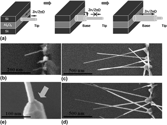
Lateral ZnO nanowires (NWs) were selectively grown from the edge of a SiO2/Si–Al2O3–SiO2/Si multilayer structure for potential integration into devices using Si processing technology. Microstructural studies demonstrate a two-step growth process in which the tip region, with a diameter of ~10 nm, rapidly grew from the Al2O3 surface and, later, a base growth with a diameter of ~22 nm overgrew the existing narrow ZnO NW, halting further tip growth. Kinetics studies showed that surface diffusion on the alumina seed surface determined ZnO NW growth rate.

Type
Articles
Copyright
Copyright © Materials Research Society 2011

Access options

Get access to the full version of this content by using one of the access options below. (Log in options will check for institutional or personal access. Content may require purchase if you do not have access.)

Footnotes

a)

Present address: Metallurgical and Materials Engineering, Center for Materials for Information Technology, The University of Alabama, Tuscaloosa, Alabama 35487

References

REFERENCES

1.Tans, S.J., Verschueren, A.R.M., and Dekker, C.: Room-temperature transistor based on a single carbon nanotube. Nature 393, 49 (1998).CrossRefGoogle Scholar
2.Duan, X.F., Huang, Y., Agarwal, R., and Lieber, C.M.: Single-nanowire electrically driven lasers. Nature 421, 241 (2003).CrossRefGoogle ScholarPubMed
3.Kong, J., Franklin, N.R., Zhou, C.W., Chapline, M.G., Peng, S., Cho, K.J., and Dai, H.J.: Nanotube molecular wires as chemical sensors. Science 287, 622 (2000).CrossRefGoogle ScholarPubMed
4.Wang, Z.L.: Zinc oxide nanostructures: Growth, properties and applications. J. Phys. Condens. Matter 16, 829 (2004).CrossRefGoogle Scholar
5.Park, J., Choi, H.H., Siebein, K., and Singh, R.K.: Two-step evaporation process for formation of aligned zinc oxide nanowires. J. Cryst. Growth 258, 342 (2003).CrossRefGoogle Scholar
6.Huang, M.H., Mao, S., Feick, H., Yan, H.Q., Wu, Y.Y., Kind, H., Weber, E., Russo, R., and Yang, P.D.: Room-temperature ultraviolet nanowire nanolasers. Science 292, 1897 (2001).CrossRefGoogle ScholarPubMed
7.Xu, F., Yuan, Z.Y., Du, G.H., Ren, T.Z., Bouvy, C., Halasa, M., and Su, B.L.: Simple approach to highly oriented ZnO nanowire arrays: Large-scale growth, photoluminescence and photocatalytic properties. Nanotechnology 17, 588 (2006).CrossRefGoogle Scholar
8.Comini, E., Faglia, G., Sberveglieri, G., Pan, Z.W., and Wang, Z.L.: Stable and highly sensitive gas sensors based on semiconducting oxide nanobelts. Appl. Phys. Lett. 81, 1869 (2002).CrossRefGoogle Scholar
9.Jeong, M.C., Oh, B.Y., Nam, O.H., Kim, T., and Myoung, J.M.: Three-dimensional ZnO hybrid nanostructures for oxygen sensing application. Nanotechnology 17, 526 (2006).CrossRefGoogle Scholar
10.Huang, M.H., Wu, Y.Y., Feick, H., Tran, N., Weber, E., and Yang, P.D.: Catalytic growth of zinc oxide nanowires by vapor transport. Adv. Mater. (Deerfield Beach Fla.) 13, 113 (2001).3.0.CO;2-H>CrossRefGoogle Scholar
11.Yang, P.D., Yan, H.Q., Mao, S., Russo, R., Johnson, J., Saykally, R., Morris, N., Pham, J., He, R.R., and Choi, H.J.: Controlled growth of ZnO nanowires and their optical properties. Adv. Funct. Mater. 12, 323 (2002).3.0.CO;2-G>CrossRefGoogle Scholar
12.Greyson, E.C., Babayan, Y., and Odom, T.W.: Directed growth of ordered arrays of small-diameter ZnO nanowires. Adv. Mater. (Deerfield Beach Fla.) 16, 1348 (2004).CrossRefGoogle Scholar
13.Fan, H.J., Fuhrmann, B., Scholz, R., Syrowatka, F., Dadgar, A., Krost, A., and Zacharias, M.: Well-ordered ZnO nanowire arrays on GaN substrate fabricated via nanosphere lithography. J. Cryst. Growth 287, 34 (2006).CrossRefGoogle Scholar
14.Heo, Y.W., Varadarajan, V., Kaufman, M., Kim, K., Norton, D.P., Ren, F., and Fleming, P.H.: Site-specific growth of Zno nanorods using catalysis-driven molecular-beam epitaxy. Appl. Phys. Lett. 81, 3046 (2002).CrossRefGoogle Scholar
15.Zhu, Z.M., Chen, T.L., Gu, Y., Warren, J., and Osgood, R.M.: Zinc oxide nanowires grown by vapor-phase transport using selected metal catalysts: A comparative study. Chem. Mater. 17, 4227 (2005).CrossRefGoogle Scholar
16.Lee, W., Jeong, M.C., and Myoung, J.M.: Evolution of the morphology and optical properties of ZnO nanowires during catalyst-free growth by thermal evaporation. Nanotechnology 15, 1441 (2004).CrossRefGoogle Scholar
17.Conley, J.F., Stecker, L., and Ono, Y.: Directed assembly of ZnO nanowires on a Si substrate without a metal catalyst using a patterned ZnO seed layer. Nanotechnology 16, 292 (2005).CrossRefGoogle Scholar
18.Wang, L.S., Zhang, X.Z., Zhao, S.Q., Zhou, G.Y., Zhou, Y.L., and Qi, J.J.: Synthesis of well-aligned ZnO nanowires by simple physical vapor deposition on c-oriented ZnO thin films without catalysts or additives. Appl. Phys. Lett. 86, 024108 (2005).CrossRefGoogle Scholar
19.Jie, J.S., Wang, G.Z., Chen, Y.M., Han, X.H., Wang, Q.T., Xu, B., and Hou, J.G.: Synthesis and optical properties of well-aligned ZnO nanorod array on an undoped ZnO film. Appl. Phys. Lett. 86, 031909 (2005).CrossRefGoogle Scholar
20.Sekar, A., Kim, S.H., Umar, A., and Hahn, Y.B.: Catalyst-free synthesis of ZnO nanowires on Si by oxidation of Zn powders. J. Cryst. Growth 277, 471 (2005).CrossRefGoogle Scholar
21.Baxter, J.B. and Aydil, E.S.: Epitaxial growth of ZnO nanowires on a- and c-plane sapphire. J. Cryst. Growth 274, 407 (2005).CrossRefGoogle Scholar
22.Park, W.I. and Yi, G.C.: Electroluminescence in n-ZnO nanorod arrays vertically grown on p-GaN. Adv. Mater. (Deerfield Beach Fla.) 16, 87 (2004).CrossRefGoogle Scholar
23.Li, S.Y., Lin, P., Lee, C.Y., and Tseng, T.Y.: Field emission and photofluorescent characteristics of zinc oxide nanowires synthesized by a metal catalyzed vapor-liquid-solid process. J. Appl. Phys. 95, 3711 (2004).CrossRefGoogle Scholar
24.Gao, P.X., Liu, J., Buchine, B.A., Weintraub, B., Wang, Z.L., and Lee, J.L.: Bridged ZnO nanowires across trenched electrodes. Appl. Phys. Lett. 91, 142108 (2007).CrossRefGoogle Scholar
25.Law, J.B.K. and Thong, J.T.L.: Lateral ZnO nanowire growth on a planar substrate using a growth barrier. Nanotechnology 18, 055601 (2007).CrossRefGoogle Scholar
26.Qin, Y., Yang, R.S., and Wang, Z.L.: Growth of horizonatal ZnO nanowire arrays on any substrate. J. Phys. Chem. C 112, 18734 (2008).CrossRefGoogle Scholar
27.Lee, J.S., Islam, M.S., and Kim, S.: Direct formation of catalyst-free ZnO nanobridge devices on an etched Si substrate using a thermal evaporation method. Nano Lett. 6, 1487 (2006).CrossRefGoogle Scholar
28.Tang, H., Chang, J.C., Shan, Y., Ma, D.D.D., Lui, T.-Y., Zapien, J.A., Lee, C.-S., and Lee, S.-T.: Growth mechanism of ZnO nanowires via direct Zn evaporation. J. Mater. Sci. 44, 563 (2008).CrossRefGoogle Scholar
29.Pan, Z.W., Budai, J.D., Dai, Z.R., Liu, W.J., Paranthaman, M.P., and Dai, S.: Zinc oxide microtowers by vapor phase homoepitaxial regrowth. Adv. Mater. (Deerfield Beach Fla.) 21, 890 (2009).CrossRefGoogle Scholar
30.Chopra, N., Kichambare, P.D., Andrews, R., and Hinds, B.J.: Control of multiwalled carbon nanotube diameter by selective growth on the exposed edge of a thin film multilayer structure. Nano Lett. 2, 1177 (2002).CrossRefGoogle Scholar
31.Chopra, N., Xu, W.T., De Long, L.E., and Hinds, B.J.: Incident angle dependence of nanogap size in suspended carbon nanotube shadow lithography. Nanotechnology 16, 133 (2005).CrossRefGoogle Scholar
32.Lefebvre, J., Radosavljevic, M., and Johnson, A.T.: Fabrication of nanometer size gaps in a metallic wire. Appl. Phys. Lett. 76, 3828 (2000).CrossRefGoogle Scholar
33.Hausmann, D., Becker, J., Wang, S.L., and Gordon, R.G.: Rapid vapor deposition of highly conformal silica nanolaminates. Science 298, 402 (2002).CrossRefGoogle ScholarPubMed
34.Elam, J.W., Sechrist, Z.A., and George, S.M.: ZnO/Al2O3 nanolaminates fabricated by atomic layer deposition: Growth and surface-roughness measurements. Thin Solid Films 414, 43 (2002).CrossRefGoogle Scholar
35.Hoivik, N.D., Elam, J.W., Linderman, R.J., Bright, V.M., George, S.M., and Lee, Y.C.: Atomic layer deposited protective coatings for microelectromechanical systems. Sens. Actuators A A103, 100 (2003).CrossRefGoogle Scholar
36.Gao, K.Y., Seyller, T., Ley, L., Ciobanu, F., Pensl, G., Tadich, A., Riley, J.D., and Leckey, R.G.C.: Al2O3 prepared by atomic layer deposition as gate dielectric on 6H-SiC(0001). Appl. Phys. Lett. 83, 1830 (2003).CrossRefGoogle Scholar
37.Hu, B., Yao, J.Y., and Hinds, B.J.: Nanogap electrodes formed at the exposed edge of Au/self-assembled monolayer/Al2O3/Au tunnel structures grown by atomic layer deposition. Appl. Phys. Lett. 97, 203111 (2010).CrossRefGoogle Scholar
38.Cha, S.N., Song, B.G., Jang, J.E., Jung, J.E., Han, I.T., Ha, J.H., Hong, J.P., Kang, D.J., and Kim, J.M.: Controlled growth of vertically aligned ZnO nanowires with different crystal orientation of the ZnO seed layer. Nanotechnology 19, 235601 (2008).CrossRefGoogle ScholarPubMed
39.Roy, V.A.L., Djurisic, A.B., Chan, W.K., Gao, J., Lui, H.F., and Surya, C.: Luminescent and structural properties of ZnO nanorods prepared under different conditions. Appl. Phys. Lett. 83, 141 (2003).CrossRefGoogle Scholar
40.Kim, H. and Sigmund, W.: ZnO nanocrystals synthesized by physical vapor deposition. J. Nanosci. Nanotechnol. 4, 275 (2004).CrossRefGoogle ScholarPubMed
41.Feng, L., Cheng, C., Lei, M., Wang, N., and Loy, M.M.T.: Spatially resolved photoluminescence study of single ZnO tetrapods. Nanotechnology 19, 405702 (2008).CrossRefGoogle ScholarPubMed
42.Kim, D.S., Gosele, U., and Zacharias, M.: Surface-diffusion induced growth of ZnO nanowires. J. Cryst. Growth 311, 3216 (2009).CrossRefGoogle Scholar
43.Rackauskas, S., Nasibulin, A.G., Jiang, H., Tian, Y., Statkute, G., Shandakov, S.D., Lipsanen, H., and Kauppinen, E.I.: Mechanistic investigation of ZnO nanowire growth. Appl. Phys. Lett. 95, 183114 (2009).CrossRefGoogle Scholar
44.Wagner, R.S. and Ellis, W.C.: Vapor-liquid-solid mechanism of single crystal growth (new method growth catalysis from impurity whisker epitaxial + large crystals Si E). Appl. Phys. Lett. 4, 89 (1964).CrossRefGoogle Scholar
45.Brenner, S.S. and Sears, G.W.: Mechanism of whisker growth—III. Nature of growth sites. Acta Metall. Mater. 4, 268 (1956).CrossRefGoogle Scholar
46.Heo, Y.W., Ip, K., Pearton, S.J., Norton, D.P., and Budai, J.D.: Growth of ZnO thin films on c-plane Al2O3 by molecular beam epitaxy using ozone as an oxygen source. Appl. Surf. Sci. 252, 7442 (2006).CrossRefGoogle Scholar