Hostname: page-component-745bb68f8f-grxwn Total loading time: 0 Render date: 2025-01-24T13:22:03.512Z Has data issue: false hasContentIssue false

Se-doped Ge10Sb90 for highly reliable phase-change memory with low operation power

Published online by Cambridge University Press:  22 June 2017
Jeong Hoon Kim
Affiliation:
Department of Materials Science and Engineering, Yonsei University, Seoul 120-749, Republic of Korea
Dae-Seop Byeon
Affiliation:
Department of Materials Science and Engineering, Yonsei University, Seoul 120-749, Republic of Korea
Dae-Hong Ko*
Affiliation:
Department of Materials Science and Engineering, Yonsei University, Seoul 120-749, Republic of Korea
Jeong Hee Park
Affiliation:
Process Development Team, Semiconductor R&D Division, Samsung Electronics Co., Ltd., Hwasung-City, Kyungki-Do 445-701, Korea
*
a)Address all correspondence to this author. e-mail: [email protected]
Get access

Abstract

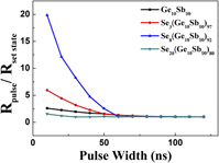
In this study, we propose a Se-incorporated Ge10Sb90 as a phase-change material for phase-change memory (PCM) with high reliability and low operation power. We investigated the effect of the Se concentration on the thermal and electrical properties of Se-doped Ge10Sb90 films by varying the Se concentration from 0 to 20 at.%. The crystallization temperature, crystallization activation energy, and maximum ten-year data retention temperature increased with the increasing Se, thus demonstrating the improved thermal stability of Se-doped Ge10Sb90 films with higher Se contents. More Se also increased the rate factor, band gap, threshold voltage, and load resistance. In addition, the crystallization speed, programming window, and resistances of both the amorphous and crystalline states increased with the increasing Se concentration. In contrast, the reset current decreased with the increasing Se concentration. These results demonstrate that Se-doped Ge10Sb90 is a highly promising material for PCM applications.

Type
Invited Papers
Copyright
Copyright © Materials Research Society 2017 

Access options

Get access to the full version of this content by using one of the access options below. (Log in options will check for institutional or personal access. Content may require purchase if you do not have access.)

Footnotes

Contributing Editor: Don W. Shaw

References

REFERENCES

Kryder, M.H. and Kim, C.S.: After hard drives-what comes next? IEEE Trans. Magn. 45, 3406 (2009).Google Scholar
Simpson, R.E., Krbal, M., Fons, P., Kolobov, A.V., Tominaga, J., Uruga, T., and Tanida, H.: Toward the ultimate limit of phase change in Ge2Sb2Te5 . Nano Lett. 10, 414 (2010).CrossRefGoogle ScholarPubMed
Ahn, S.J., Hwang, Y.N., Song, Y.J., Lee, S.H., Lee, S.Y., Park, J.H., Jeong, C.W., Ryoo, K.C., Shin, J.M., Park, J.H., Fai, Y., Oh, J.H., Koh, G.H., Jeong, G.T., Joo, S.H., Choi, S.H., Son, Y.H., Shin, J.C., Kim, Y.T., Jeong, H.S., and Kim, K.: Highly reliable 50 nm contact cell technology for 256 Mb PRAM. In Symposium on VLSI Technology Digest of Technical Papers (IEEE Symposium on VLSI Technology, Kyoto, Japan, 2005); pp. 9899.Google Scholar
Cho, S.L., Yi, J.H., Ha, Y.H., Kuh, B.J., Lee, C.M., Park, J.H., Nam, S.D., Horii, H., Cho, B.O., Ryoo, K.C., Park, S.O., Kim, H.S., Chung, U.I., Moon, J.T., and Ryu, B.I.: Highly scalable on-axis confined cell structure for high density PRAM beyond 256 Mb. In Symposium on VLSI Technology Digest of Technical Papers (IEEE Symposium on VLSI Technology, Kyoto, Japan, 2005); pp. 9697.Google Scholar
Xiong, F., Bae, M.H., Dai, Y., Liao, A.D., Behnam, A., Carrion, E.A., Hong, S., Ielmini, D., and Pop, E.: Self-aligned nanotube-nanowire phase change memory. Nano Lett. 13, 464 (2013).Google Scholar
Nam, S-W., Chung, H-S., Lo, Y.C., Qi, L., Li, J., Lu, Y., Johnson, A.T.C., Jung, Y.W., Nukala, P., and Agarwal, R.: Electrical wind force-driven and dislocation-templated amorphization in phase-change nanowires. Science 336, 1561 (2012).CrossRefGoogle ScholarPubMed
Terao, M., Morikawa, T., and Ohta, T.: Electrical phase-change memory: Fundamentals and state of the art. Jpn. J. Appl. Phys. 48, 080001 (2009).Google Scholar
Loke, D., Lee, T.H., Wang, W.J., Shi, L.P., Zhao, R., Yeo, Y.C., Chong, T.C., and Elliott, S.R.: Breaking the speed limits of phase-change memory. Science 336, 1566 (2012).CrossRefGoogle ScholarPubMed
Lai, S. and Lowrey, T.: OUM-A 180 nm nonvolatile memory cell element technology for stand alone and embedded applications. In IEEE IEDM Tech. Dig. (IEEE International Electron Devices Meeting, Washington, DC, 2001); pp. 36.5.136.5.4.Google Scholar
Takaura, N., Ohyanagi, T., Tai, M., Kitamura, M., Kinoshita, M., Akita, K., Morikawa, T., Kato, S., Araidai, M., Kamiya, K., Yamamoto, T., and Shiraishi, K.: Understanding the switching mechanism of charge-injection GeTe/Sb2Te3 phase change memory through electrical measurement and analysis of 1R test structure. In ICMTS (IEEE International Conference, Udine, Italy, 2014); pp. 3237.Google Scholar
Hosaka, S., Tamura, K.M., Sone, H., and Koyanagi, H.: Proposal for a memory transistor using phase-change and nanosize effects. Microelectron. Eng. 73–74, 736 (2004).Google Scholar
Maimon, J.D., Hunt, K.K., Burcin, L., and Rodgers, J.: Chalcogenide memory arrays: Characterization and radiation effects. IEEE Trans. Nucl. Sci. 50, 1878 (2003).Google Scholar
Van Pieterson, L., Lankhrst, M.H.R., Van Schijndel, M., Kuiper, A.E.T., and Roosen, J.H.J.: Phase change recording materials with a growth-dominated crystallization mechanism: A materials overview. J. Appl. Phys. 97, 083520 (2005).Google Scholar
Cheng, H.Y., Hsu, T.H., Raoux, S., Wu, J.Y., Du, P.Y., Breitwisch, M., Zhu, Y., Lai, E.K., Joseph, E., Mittal, S., Cheek, R., Schrott, A., Lai, S.C., Lung, H.L., and Lam, C.: A high performance phase change memory with fast switching speed and high temperature retention by engineering the Ge x Sb y Te z phase change material. Presented at the Electron Devices Meeting, IEDM 2011 (IEEE International, Washington, DC, 2011); pp. 3.4.13.4.4.Google Scholar
Rauox, S., Cheng, H-Y., Sandrini, J., Li, J., and Jordan-Sweet, J.: Materials engineering for phase change random access memory. In Non-Volatile Memory Technology Symposium (NVMTS), 2011 11th Annual (IEEE, Shanghai, China, 2011); pp. 15.Google Scholar
Kang, M.J., Park, T.J., Wamwangi, D., Wang, K., Steimer, C., Choi, S.Y., and Wuttig, M.: Electrical properties and crystallization behavior of Sb x Se100−x thin films. Microsyst. Technol. 13, 153 (2007).Google Scholar
Kang, M.J., Choi, S.Y., Wamwangi, D., Wang, K., Steimer, C., and Wuttig, M.: Structural transformation of Sb x Se100−x thin films for phase change nonvolatile memory applications. J. Appl. Phys. 98, 014904 (2005).Google Scholar
Giridhar, A., Narasimham, P.S.L., and Mahadevan, S.: Electrical properties of GeSbSe glasses. J. Non-Cryst. Solids 37, 165 (1980).Google Scholar
Saleh, S.A.: Synthesis and characterization of Sb65Se35−x Ge x alloys. Mater. Sci. Appl. 2, 950 (2011).Google Scholar
Zachariasen, W.H.: The atomic arrangement in glass. J. Am. Chem. Soc. 54, 3841 (1932).CrossRefGoogle Scholar
Pauling, L.: The Nature of the Chemical Bond and the Structure of Molecules and Crystals: An Introduction to Modern Structural Chemistry, 3rd ed. (Cornell University, New York, 1960); ch. 3.Google Scholar
Kissinger, H.E.: Reaction kinetics in differential thermal analysis. Anal. Chem. 29, 1702 (1957).Google Scholar
Chang, P.C., Chang, C.C., Chang, S.C., and Chin, T.S.: Crystallization behavior of Si-added amorphous Ga19Sb81 films for phase-change memory. J. Non-Cryst. Solids 383, 106 (2014).CrossRefGoogle Scholar
Cheng, H.Y., Kao, K.F., Lee, C.M., and Chin, T.S.: Crystallization kinetics of Ga–Sb–Te films for phase change memory. Thin Solid Films 516, 5513 (2008).Google Scholar
Johnson, W.A. and Mehl, R.F.: Reaction kinetics in processes of nucleation and growth. Trans. Am. Inst. Min., Metall. Pet. Eng. 135, 416 (1939).Google Scholar
Lee, H., Kim, Y.K., Kim, D., and Kang, D.H.: Switching behavior of indium selenide based phase-change memory cell. IEEE Trans. Magn. 41, 1034 (2005).Google Scholar
Feng, J., Zhang, Y., Cai, B., and Chen, B.: Thermal stability and electronic structures of N-doped SiSb films for high temperature applications of phase-change memory. Appl. Phys. A 97, 507 (2009).Google Scholar
Hwang, Y.N., Lee, S.H., Ahn, S.J., Lee, S.Y., Ryoo, K.C., Hong, H.S., Koo, H.C., Yeung, F., Oh, J.H., Kim, H.J., Jeong, W.C., Park, J.H., Horii, H., Ha, Y.H., Yi, J.H., Koh, G.H., Jeong, G.T., Jeong, H.S., and Kim, K.N.: Writing current reduction for high-density phase-change RAM. In IEEE IEDM Tech. Dig. (IEEE International Electron Devices Meeting, Washington, DC, 2003); pp. 37.1.137.1.4.Google Scholar
Madelung, O., Rössler, U., and Schulz, M.: Non-Tetrahedrally Bonded Elements and Binary Compounds I, 1st ed. (Springer, Heidelberg, 1998).Google Scholar
Bhatnagar, A.K., Reddy, K.V., and Srivastava, V.: Optical energy gap of amorphous selenium: Effect of annealing. J. Phys. D: Appl. Phys. 18, L149 (1985).Google Scholar
Zhou, X., Wu, L., Song, Z., Rao, F., Zhu, M., Peng, C., Yao, D., Song, S., Liu, B., and Feng, S.: Carbon-doped Ge2Sb2Te5 phase change material: A candidate for high-density phase change memory application. Appl. Phys. Lett. 101, 142104 (2012).CrossRefGoogle Scholar
Do, K.H., Lee, D.K., Sohn, H.C., Cho, M-H., and Ko, D-H.: Crystallization behaviors of laser induced Ge2Sb2Te5 in different amorphous states. J. Electrochem. Soc. 157, H264 (2010).Google Scholar
Do, K.H., Lee, D.K., Bae, J-H., Ko, D-H., Sohn, H.C., and Cho, M-H.: Comparison of the crystallization behaviors in as-deposited and melt-quenched N-doped Ge2Sb2Te5 Thin films. J. Electrochem. Soc. 158, H347 (2011).Google Scholar
Supplementary material: Image

Kim supplementary material

Kim supplementary material

Download Kim supplementary material(Image)
Image 24.9 KB