Hostname: page-component-586b7cd67f-dlnhk Total loading time: 0 Render date: 2024-11-23T01:28:31.725Z Has data issue: false hasContentIssue false

Phase transformation in self-assembled Gd silicide nanostructures on Si(001)

Published online by Cambridge University Press:  30 June 2011

Gangfeng Ye
Affiliation:
Department of Chemical Engineering and Materials Science, Michigan State University, East Lansing, Michigan, 48824-1226
Martin A. Crimp
Affiliation:
Department of Chemical Engineering and Materials Science, Michigan State University, East Lansing, Michigan, 48824-1226
Jun Nogami*
Affiliation:
Department of Materials Science and Engineering, University of Toronto, Toronto, Ontario, Canada M5S 3E4
*
b)Address all correspondence to this author. e-mail: [email protected]
Get access

Abstract

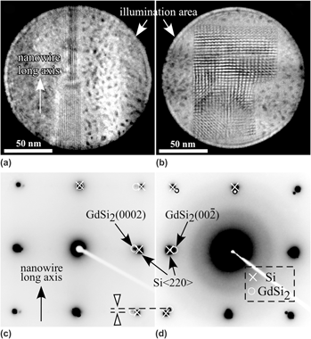
Gd silicide nanostructures epitaxially grown on Si(001) are studied by plan-view transmission electron microscopy and associated nanobeam electron diffraction, as well as scanning tunneling microscopy. The nanobeam diffraction measurements show a direct correlation between the nanostructure morphology, either nanowires or islands, and the silicide crystal structure. Scanning tunneling microscopy shows a phase transformation from nanowires to islands that nucleate at nanowire intersections. A specific mechanism for this transformation is proposed that explains nanowire growth behavior previously observed on vicinal Si surfaces.

Type
Articles
Copyright
Copyright © Materials Research Society 2011

Access options

Get access to the full version of this content by using one of the access options below. (Log in options will check for institutional or personal access. Content may require purchase if you do not have access.)

Footnotes

a)

Present address: Nanolab Technologies, San Jose, California 95134

References

REFERENCES

1.Preinesberger, C., Vandré, S., Kalka, T., and Dähne-Prietch, M.: Formation of dyprosium silicide wires on Si(001). J. Phys. D: Appl. Phys. 31, L43 (1998).Google Scholar
2.Chen, Y., Ohlberg, D.A.A., Medeiros-Ribeiro, G., Chang, Y.A., and Williams, R.S.: Self-assembled growth of epitaxial erbium disilicide nanowires. Appl. Phys. Lett. 76, 4004 (2000).Google Scholar
3.Nogami, J., Liu, B.Z., Katkov, M.V., Ohbuchi, C., and Birge, N.O.: Self-assembled rare earth silicide nanowires on Si(001). Phys. Rev. B 63, 233305 (2001).Google Scholar
4.Eames, C., Reakes, M., Tear, S.P., Noakes, T.C.Q., and Bailey, P.: Phase selection in the rare earth silicides. Phys. Rev. B 82, 174112 (2010).CrossRefGoogle Scholar
5.Houssay, E., Rouault, A., Thomas, O., Madar, R., and Senateur, J.P.: Metallurgical reinvestigation of rare earth silicides. Appl. Surf. Sci. 38, 156 (1989).Google Scholar
6.Liu, B.Z. and Nogami, J.: An STM study of dysprosium silicide nanowire growth on Si(001). J. Appl. Phys. 93, 593 (2003).CrossRefGoogle Scholar
7.Ye, G., Nogami, J., and Crimp, M.A.: Dysprosium disilicide nanostructures on silicon(001) studied by scanning tunneling microscopy and transmission electron microscopy. Thin Solid Films 497, 48 (2006).CrossRefGoogle Scholar
8.Ye, G., Crimp, M.A., and Nogami, J.: Crystallographic study of self-assembled dysprosium silicide nanostructures on Si(001). Phys. Rev. B 74, 033104 (2006).CrossRefGoogle Scholar
9.Zhang, J., Crimp, M.A., Cui, Y., and Nogami, J.: Self-assembled thulium silicide nanostructures on silicon(001) studied by scanning tunneling microscopy and transmission electron microscopy. J. Appl. Phys. 103, 064308 (2008).CrossRefGoogle Scholar
10.Lee, D. and Kim, S.: Formation of hexagonal Gd disilicide nanowires on Si(100). Appl. Phys. Lett. 82, 2619 (2003).Google Scholar
11.Harrison, B.C., and Boland, J.J.: Real-time STM study of inter-nanowire reactions: GdSi2 nanowires on Si(1 0 0). Surf. Sci. 594, 93 (2005).CrossRefGoogle Scholar
12.Ye, G., Crimp, M.A., and Nogami, J.: Self-assembled GdSi2 nanostructures grown on Si(001) studied by TEM and STM. in Assembly at the Nanoscale – Toward Functional Nanostructured Materials, edited by Ozkan, C.S., Rosei, F., Lopinski, G.P., and Wang, Z.L. (Mater. Res. Soc. Symp. Proc. 901 E, Warrendale, PA, 2006), 0901-Ra13-05.Google Scholar
13.Molnar, G., Gerocs, I., Peto, G., Zsoldos, E., Jaroli, E., and Gyulai, J.: Thickness-dependent formation of Gd-silicide compounds. J. Appl. Phys. 64, 6746 (1988).Google Scholar
14.Wierenga, P.E., Kubby, J.A., and Griffith, J.E.: Tunneling Images of Biatomic Steps on Si(100). Phys. Rev. Lett. 59, 2169 (1987).CrossRefGoogle Scholar
15.Liu, B.Z. and Nogami, J.: Growth of parallel rare earth silicide nanowire arrays on vicinal Si(001). Nanotechnology 14, 873 (2003).CrossRefGoogle Scholar
16.Yeom, H.W., Kim, Y.K., Lee, E.Y., Ryang, K.-D., and Kang, P.G.: Robust one-dimensional metallic band structure of silicide nanowires. Phys. Rev. Lett. 95, 205504 (2005).CrossRefGoogle ScholarPubMed
17.Lee, D., Kim, D.K., Bae, S.S., Kim, S., Ragan, R., Ohlberg, D.A.A., Chen, Y., and Williams, R.S.: Unidirectional hexagonal rare-earth disilicide nanowires on vicinal Si(100)-2×1. Appl. Phys. A: 80, 1311 (2005).Google Scholar