Hostname: page-component-745bb68f8f-g4j75 Total loading time: 0 Render date: 2025-01-09T22:03:57.031Z Has data issue: false hasContentIssue false

Optical reflectance of alkali-textured silicon wafers with pyramidal facets: 2D analytical model

Published online by Cambridge University Press:  16 April 2015
Adebayo Adeboye Fashina
Affiliation:
Department of Theoretical and Applied Physics, African University of Science and Technology, PMB 681, Garki, Abuja, Nigeria
Martiale Gaetan Zebaze Kana
Affiliation:
Physics Advanced Laboratory, Sheda Science and Technology Complex, PMB 186, Garki, Abuja, Nigeria; and Department of Materials Science and Engineering, Kwara State University, PMB 1530, Malate, Nigeria
Winston Oluwole Soboyejo*
Affiliation:
Department of Theoretical and Applied Physics, African University of Science and Technology, PMB 681, Garki, Abuja, Nigeria; Department of Mechanical and Aerospace Engineering, Princeton University, Princeton, New Jersey 08544, USA; and Princeton Institute of Science and Technology of Materials (PRISM), Bowen Hall, Princeton, New Jersey 08544, USA
*
a)Address all correspondence to this author. e-mail: [email protected]
Get access

Abstract

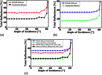
This study presents an analytical model of the reflectance of flat and textured silicon substrates. The model was used to study the reflection behavior of textured silicon surfaces under non-normal incidence. By characterizing the incident light and facets of the silicon wafer with vector geometry, dot products and Phong's reflection model (https://cs.oberlin.edu/∼bob/cs357.08/VectorGeometry/VectorGeometry.pdf) were used to determine the reflection angles between incident light rays and pyramidal facets. The possible optical interactions are considered for a wide range of pyramidal geometries and light incidence angles that are relevant to the exposure of textured silicon surfaces to incident sunlight. Furthermore, the model was used to investigate the possibility of secondary reflection, for the full range of incidence angles to the substrate. The textured silicon surfaces were found to reduce the reflection angles more effectively than flat substrates at lower angles of incidence. Secondary reflection was also found to be experienced or guaranteed, for all pyramid heights, when the angle of incidence to the substrate was less than 19.4°. The predictions are validated with experimental measurements of reflectance from (001)-textured silicon surfaces. The implications of the results are then discussed for the development of micropyramids for improved photoconversion in silicon solar cells.

Type
Articles
Copyright
Copyright © Materials Research Society 2015 

Access options

Get access to the full version of this content by using one of the access options below. (Log in options will check for institutional or personal access. Content may require purchase if you do not have access.)

References

REFERENCES

Chung, H., Chen, C., and Chu, H.: Analysis of pyramidal surface texturization of silicon solar cells by molecular dynamics simulations. Int. J. Photoenergy 2008, 16 (2008).Google Scholar
Gee, J.M., Gordon, R., and Laing, H.F.: Optimization of textured-dielectric coatings for crystalline-silicon solar cells. In Proceedings of the 25th IEEE Photovoltaic Specialists Conference, Washington DC, 1996; pp. 733736.Google Scholar
Hylton, J.D., Burgers, A.R., and Sinke, W.C.: Alkaline etching for reflectance reduction in multicrystalline silicon solar cells. J. Electrochem. Soc. 151(6), 408427 (2004).CrossRefGoogle Scholar
Tellier, C.R. and Brahim-Bounab, A.: Anisotropic etching of silicon crystals in KOH solution. J. Mater. Sci. 29(22), 59535971 (1994).CrossRefGoogle Scholar
Shikida, M., Sato, K., Tokoro, K., and Uchikawa, D.: Differences in anisotropic etching properties of KOH and TMAH solution. Sens. Actuators, A 80, 179188 (1999).CrossRefGoogle Scholar
Seidal, H., Csepregi, L., Henberger, A., and Baumgartel, H.: Anisotropic etching of crystalline silicon in alkaline solutions. J. Electrochem. Soc. 137(11), 116125 (1990).Google Scholar
Kilpinen, P., Haimi, E., and Lindroos, V.K.: The etch rate variations of p+ silicon wafers in aqueous KOH solutions as a function of processing conditions. MRS Proc. 605, 293 (1999). doi:10.1557/PROC-605-293.CrossRefGoogle Scholar
Seidal, H., Csepregi, L., Henberger, A., and Baumgartel, H.: Anisotropic etching of crystalline silicon in alkaline solution: Orientation dependence and behavior of passivation layers. J. Electrochem. Soc. 137(11), 612626 (1996).Google Scholar
Sato, K., Shikida, M., Yamashiro, T., Tsunekawa, M., and Ito, S.: Roughening of single-crystal silicon surface etched by KOH water solutions. Sens. Actuators, A 73, 122130 (1999).CrossRefGoogle Scholar
Kassel, L.E.: KOH-etch related defects on processed silicon wafers. MRS Proc. 259, 187 (1992). doi:10.1557/PROC-259-187.CrossRefGoogle Scholar
Yang, C., Chen, P., Chiou, Y., and Lee, R.: Effects of mechanical agitation and surfactant additive on silicon anisotropic etching in alkaline KOH solution. Sens. Actuators, A 119, 263270 (2005).CrossRefGoogle Scholar
Zubel, I. and Kramkowska, M.: The effect of isopropyl alcohol on etching rate and roughness of (100) Si surface etched in KOH and TMAH solutions. Sens. Actuators, A 93, 138147 (2001).CrossRefGoogle Scholar
Moroz, V., Huang, J., Wijekoon, K., and Tanner, D.: Experimental and theoretical analysis of the optical behavior of textured silicon wafers. In Proceedings of the 37th IEEE Photovoltaic Specialists Conference. (IEEE, Seattle, WA, 2011); pp. 29002905.Google Scholar
Zhu, X., Wang, L., and Yang, D.: Investigations of random pyramid texture on the surface of single-crystalline silicon for solar cells. In Proceedings of the ISES Solar World Congress, Beijing, China, (Springer-Verlag, Berlin Heidelberg, Germany, 2007); pp. 11261130.Google Scholar
Campbell, P. and Green, M.A.: Light trapping properties of pyramidally textured surfaces. J. Appl. Phys. 62(1), 243249 (1987).CrossRefGoogle Scholar
Baker‐Finch, S.C. and McIntosh, K.R.: Reflection distributions of textured monocrystalline silicon: Implications for silicon solar cells. Prog. Photovoltaics Res. Appl. 21(5), 960971 (2013). DOI: 10.1002/pip.2186.CrossRefGoogle Scholar
Baker‐Finch, S.C. and McIntosh, K.R.: Reflection of normally incident light from silicon solar cells with pyramidal texture. Prog. Photovoltaics Res. Appl. 19(4), 406416 (2011). DOI: 10.1002/pip.1050.CrossRefGoogle Scholar
O'Mara, W.C., Herring, R.B., and Hunt, L.P.: Handbook of Semiconductor Silicon Technology (William Andrew Inc., Norwich, NY, 1990); pp. 349352.Google Scholar
King, D.L. and Buck, M.E.: Experimental optimization of an anisotropic etching process for random texturization of silicon solar cells. In Proceedings of the 22nd IEEE Photovoltaic Specialists Conference, 1991; pp. 303308.Google Scholar
Parretta, A., Sarno, A., Tortora, P., Yakubu, H., Maddalena, P., Zhao, J., and Wang, A.: Angle dependent reflectance measurements on photovoltaic materials and solar cells. Opt. Commun. 172(1–6), 139151 (1999).CrossRefGoogle Scholar
Dziuban, J.A.: Bonding in Microsystem Technology (Springer, Science & Business Media, 2007); p. 16.Google Scholar
Baker-Finch, S.C.: Rules and tools for understanding, modelling and designing textured silicon solar cells. Ph.D. Thesis, Australia National University, 2012.CrossRefGoogle Scholar
Geitz, B.: Vector Geometry for Computer Graphics. e-Publishing, Part III (2007); pp. 1516. [Online]. Available: https://cs.oberlin.edu/∼bob/cs357.08/VectorGeometry/VectorGeometry.pdf (Accessed August 25, 2013).Google Scholar
Wijekoon, K., Weidman, T., Paak, S., and MacWilliams, K.: Production ready novel texture etching process for fabrication of single crystalline silicon solar cells. In Proceedings of the 35th IEEE Photovoltaic Specialists Conference, Honolulu, HI, 2010; pp. 36353641.Google Scholar
Bressers, P.M.M., Kelly, J.J., Gardeniers, J.G.E., and Elwenspoek, M.: Surface morphology of p-type (100) silicon etched in aqueous alkaline solution. J. Electrochem. Soc. 143(5), 17441750 (1996).CrossRefGoogle Scholar
Wu, C.J., Wei, P.J., and Lin, J.F.: The reflectivity of an etched silicon surface with pyramids: I. Theoretical model and its predictions. J. Micromech. Microeng. 19, 17 (2009).Google Scholar
Singh, P.K., Kumar, R., Lal, M., Singh, S.N., and Das, B.K.: Effectiveness of anisotropic etching of silicon in aqueous alkaline solution. Sol. Energy Mater. Sol. Cells 70, 102113 (2001).CrossRefGoogle Scholar
Pedrotti, F.L., Pedrotti, L.S., and Pedrotti, L.M.: Introduction to Optics, 3rd ed. (Pearson Prentice Hall, Upper Saddle River, NJ, 2007).Google Scholar
Hamel, A. and Chibani, A.: Characterization of texture surface for solar cells. J. Appl. Phys. 10(3), 231234 (2010).Google Scholar
Xi, Z., Yang, D., Dan, W., Jun, C., Li, X., and Que, D.: Texturization of cast multicrystalline silicon for solar cells. Semicond. Sci. Technol. 19(3), 485489 (2004).CrossRefGoogle Scholar
Sethi, C., Anand, V.K., Walia, K., and Sood, S.C.: Optimization of surface reflectance for alkaline textured monocrystalline silicon solar cell. IJCSCT 5(1), 785788 (2012).Google Scholar
McIntosh, K.R. and Baker‐Finch, S.C.: OPAL 2: Rapid optical simulation of silicon solar cells. In Proceedings of the 38th IEEE Photovoltaic Specialists Conference, Austin, TX, 2012; pp. 265271. DOI: 10.1109/PVSC.2012.6317616.Google Scholar
Baker‐Finch, S.C. and McIntosh, K.R.: A freeware program for precise optical analysis of the front surface of a solar cell. In Proceedings of the 35th IEEE Photovoltaic Specialists Conference, Honolulu, HI, 2010; pp. 21842187. DOI: 10.1109/PVSC.2010.5616132.Google Scholar