Hostname: page-component-586b7cd67f-2brh9 Total loading time: 0 Render date: 2024-11-23T06:56:07.077Z Has data issue: false hasContentIssue false

Observation of compound semiconductors and heterovalent interfaces using aberration-corrected scanning transmission electron microscopy

Published online by Cambridge University Press:  30 August 2016

David J. Smith*
Affiliation:
Department of Physics, Arizona State University, Tempe, AZ 85287, USA; and Center for Photonic Innovation, Arizona State University, Tempe, AZ 85287, USA
Jing Lu
Affiliation:
Center for Photonic Innovation, Arizona State University, Tempe, AZ 85287, USA; and School of Engineering for Matter, Transport and Energy, Arizona State University, Tempe, AZ 85287, USA
Toshihiro Aoki
Affiliation:
LeRoy Eyring Center for Solid State Science, Arizona State University, Tempe, AZ 85287, USA
Martha R. McCartney
Affiliation:
Department of Physics, Arizona State University, Tempe, AZ 85287, USA; and Center for Photonic Innovation, Arizona State University, Tempe, AZ 85287, USA
Yong-Hang Zhang
Affiliation:
Center for Photonic Innovation, Arizona State University, Tempe, AZ 85287, USA; and School of Electrical, Computer, and Energy Engineering, Arizona State University, Tempe, AZ 85287, USA
*
a)Address all correspondence to this author. e-mail: [email protected]
Get access

Abstract

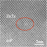
This paper reviews our recent investigations of compound semiconductors and heterovalent interfaces using the technique of aberration-corrected scanning transmission electron microscopy. Bright-field imaging of compound semiconductors with a collection angle that is comparable in size to the incident-beam convergence angle is demonstrated to provide better atomic-column visibility for lighter elements in comparison with the more traditional high-angle annular-dark-field approach. Several pairs of Group II–VI/Group III–V compound semiconductors with zincblende structure have been studied in detail. These combinations are all valence-mismatched (i.e., heterovalent), and include CdTe/InSb (Δa/a ≤ 0.05%), ZnTe/InP (Δa/a = 3.8%), and ZnTe/GaAs (Δa/a = 7.4%). CdTe/InSb (001) interfaces are observed to be defect-free with a slight lattice contraction at the interface plane. For interfaces with larger lattice-parameter mismatch, the primary interfacial defects are identified as Lomer edge dislocations and perfect 60° dislocations. However, the atomic structure of the dislocation cores has not yet been unambiguously determined.

Type
Invited Feature Paper
Copyright
Copyright © Materials Research Society 2016 

Access options

Get access to the full version of this content by using one of the access options below. (Log in options will check for institutional or personal access. Content may require purchase if you do not have access.)

Footnotes

Contributing Editor: Eric Stach

This paper has been selected as an Invited Feature Paper.

References

REFERENCES

Zhang, Y-H., Wu, S.N., Ding, D., Yu, S.Q., and Johnson, S.R.: A proposal for monolithographically integrated multijunction solar cells using lattice-matched II/VI and III/V semiconductors. Presented at the Proc. 33rd IEEE Photovoltaics Specialists Conference, 2008; pp. 15.Google Scholar
Haider, M., Uhlemann, S., Schwan, E., Rose, H., Kabius, B., and Urban, K.: Electron microscopy image enhanced. Nature 392, 768 (1998).CrossRefGoogle Scholar
Krivanek, O.L., Dellby, N., and Lupini, A.R.: Towards sub-Å electron beams. Ultramicroscopy 78, 1 (1999).CrossRefGoogle Scholar
Smith, D.J.: Development of aberration-corrected electron microscopy. Microsc. Microanal. 14, 2 (2008).CrossRefGoogle ScholarPubMed
Smith, D.J., Aoki, T., Mardinly, J., Zhou, L., and McCartney, M.R.: Exploring aberration-corrected electron microscopy for compound semiconductors. Microscopy 62(Suppl. 1), S65 (2013).Google Scholar
Wang, C., Smith, D.J., Tobin, S., Parodos, T., Zhao, J., Chang, Y., and Sivananthan, S.: Understanding ion-milling damage in Hg1−x Cd x Te epilayers. J. Vac. Sci. Technol., A 24, 995 (2006).Google Scholar
Scherzer, O.: Über einige Fehler von Elektronenlinsen (Some defects of electron lenses). Optik 101, 593 (1936).Google Scholar
Coene, W., Janssen, G., Op De Beeck, M., and van Dyck, D.: Phase retrieval through focus variation for ultra-resolution in field-emission transmission electron microscopy. Phys. Rev. Lett. 69, 3743 (1992).Google Scholar
Orchowski, A., Rau, W.D., and Lichte, H.: Electron holography surmounts resolution limit of electron microscopy. Phys. Rev. Lett. 74, 399 (1995).CrossRefGoogle ScholarPubMed
Zhou, L., Dimakis, E., Hathwar, R., Aoki, T., Smith, D.J., Moustakas, T.D., Goodnick, S.M., and McCartney, M.R.: Measurement and effects of polarization fields on one-monolayer-thick InN/GaN multiple quantum wells. Phys. Rev. B: Condens. Matter Mater. Phys. 88, 125310 (2013).Google Scholar
Pennycook, S.J., Chisholm, M.F., Lupini, A.R., Varela, M., van Benthem, K., Oxley, M.P., Luo, W., and Pantelides, S.T.: Materials applications of aberration-corrected scanning transmission electron microscopy. Adv. Imaging Electron Phys. 153, 327 (2008).Google Scholar
Findlay, S.D., Shibata, N., Sawada, H., Okunishi, E., Kondo, Y., Yamamoto, Y., and Ikuhara, Y.: Robust atomic resolution imaging of light elements using scanning transmission electron microscopy. Appl. Phys. Lett. 95, 191913 (2009).Google Scholar
Aoki, T., Lu, J., McCartney, M.R., and Smith, D.J.: Large-collection-angle bright-field imaging of compound semiconductors using aberration-corrected scanning transmission electron microscopy. Semicond. Sci. Technol. 31, 094002 (2016).CrossRefGoogle Scholar
Steenbergen, E.H., Huang, Y., Ryou, J-H., Ouyang, L., Li, J-J., Smith, D.J., Dupuis, R.D., and Zhang, Y-H.: Structural and optical characterization of type-II InAs/InAs1−x Sb x superlattices grown by metalorganic chemical vapor deposition. Appl. Phys. Lett. 99, 071111 (2011).CrossRefGoogle Scholar
Lu, J., Luna, E., Aoki, T., Steenbergen, E.H., Zhang, Y-H., and Smith, D.J.: Evaluation of antimony segregation in InAs/InAs1−x Sb x type-II superlattices grown by molecular beam epitaxy. J. Appl. Phys. 119, 095702 (2016).Google Scholar
Williams, G.M., Whitehouse, C.R., Cullis, A.G., Chew, N.G., and Blackmore, G.W.: Growth of CdTe–InSb multilayers on (100) InSb substrates using molecular beam epitaxy. Appl. Phys. Lett. 53, 1847 (1988).Google Scholar
Lu, J., DiNezza, M.J., Zhao, X-H., Liu, S., Zhang, Y-H., Kovacs, A., Dunin-Borkowski, R.E., and Smith, D.J.: Towards defect-free epitaxial CdTe and MgCdTe layers grown on InSb (001) substrates. J. Cryst. Growth 439, 99 (2016).Google Scholar
Ouyang, L., Fan, J., Wang, S., Lu, X., Zhang, Y-H., Liu, X., Furdyna, J., and Smith, D.J.: Microstructural characterization of thick ZnTe epilayers grown on GaSb, InAs, InP and GaAs (100) substrates. J. Cryst. Growth 330, 30 (2011).CrossRefGoogle Scholar