Hostname: page-component-586b7cd67f-2brh9 Total loading time: 0 Render date: 2024-11-22T21:10:41.263Z Has data issue: false hasContentIssue false

Exploring argon plasma effect on ferroelectric Hf0.5Zr0.5O2 thin film atomic layer deposition

Published online by Cambridge University Press:  05 October 2020

Jae Hur
Affiliation:
School of Electrical and Computing Engineering, Georgia Institute of Technology, Atlanta, Georgia30332, USA
Panni Wang
Affiliation:
School of Electrical and Computing Engineering, Georgia Institute of Technology, Atlanta, Georgia30332, USA
Nujhat Tasneem
Affiliation:
School of Electrical and Computing Engineering, Georgia Institute of Technology, Atlanta, Georgia30332, USA
Zheng Wang
Affiliation:
School of Electrical and Computing Engineering, Georgia Institute of Technology, Atlanta, Georgia30332, USA
Asif Islam Khan*
Affiliation:
School of Electrical and Computing Engineering, Georgia Institute of Technology, Atlanta, Georgia30332, USA
Shimeng Yu*
Affiliation:
School of Electrical and Computing Engineering, Georgia Institute of Technology, Atlanta, Georgia30332, USA
*
a)Address all correspondence to these authors. e-mail: [email protected]
Get access

Abstract

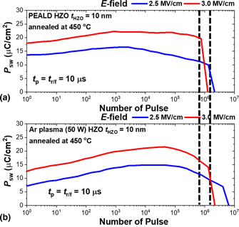
The doped/alloyed HfO2 and ZrO2 thin films revolutionized not only the field of ferroelectric physics but also various ranges of device applications. Especially when the two oxides are combined in an 1:1 ratio, the ferroelectric polarization of the material became the most distinctive. Many researchers have investigated various different process conditions such as controlling Hf0.5Zr0.5O2 (HZO) film thickness and modifying different metal electrodes. Here, we explored the effect of additional Ar plasma treatment to the HZO film. The additional Ar plasma was exposed to the plasma-enhanced atomic layer deposition (PEALD) HZO for this study. Then, the sample was compared with a conventional PEALD and thermal ALD HZO films. By understanding the polarization–electric field (P–E), current–electric field (I–E), and electrical breakdown characteristics of the different samples, it was found that the Ar plasma treatment can control the degree of ferroelectric and antiferroelectric phases of HZO film.

Type
Article
Copyright
Copyright © The Author(s), 2020, published on behalf of Materials Research Society by Cambridge University Press

Access options

Get access to the full version of this content by using one of the access options below. (Log in options will check for institutional or personal access. Content may require purchase if you do not have access.)

References

Huan, T.D.: Pathways towards ferroelectricity in hafnia. Phys. Rev. B 90, 064111-1064111-5 (2014).CrossRefGoogle Scholar
Batra, R., Huan, T.D., Rossetti, G.A., and Ramprasad, R.: Dopants promoting ferroelectricity in hafnia: Insights from a comprehensive chemical space exploration. Chem. Mater. 29, 9102 (2017).CrossRefGoogle Scholar
Lomenzo, P.D., Takmeel, Q., Zhou, C., Fancher, C.M., Lambers, E., Rudawski, N.G., Jones, J.L., Moghaddam, S., and Nishida, T.: TaN interface properties and electric field cycling effects on ferroelectric Si-doped HfO2 thin films. J. Appl. Phys. 117, 134105 (2015).CrossRefGoogle Scholar
Pešić, M. and Larcher, L.: Root Causes for Ferroelectricity in Doped HfO2 .In Ferroelectricity in Doped Hafnium Oxide: Materials, Properties and Devices, Schroeder, U., Hwang, C.S. and Funakubo, H., eds. (Woodhead Publishing, Cambridge, 2019), pp. 399411.CrossRefGoogle Scholar
Shiraishi, T., Katayama, K., Yokouchi, T., Shimizu, T., Oikawa, T., Sakata, O., Uchida, H., Imai, Y., Kiguchi, T., Konno, T.J., and Funakubo, H.: Impact of mechanical stress on ferroelectricity in (Hf0.5Zr0.5)O2 thin films. Appl. Phys. Lett. 108, 262904 (2016).CrossRefGoogle Scholar
Cheema, S.S., Kwon, D., Shanker, N., dos Reis, R., Hsu, S.-L., Xiao, J., Zhang, H., Wagner, R., Datar, A., McCarter, M.R., Serrao, C.R., Yadav, A.K., Karbasian, G., Hsu, C.-H., Tan, A.J., Wang, L.-C., Thakare, V., Zhang, X., Mehta, A., Karapetrova, E., Chopdekar, R.V., Shafer, P., Arenholz, E., Hu, C., Proksch, R., Ramesh, R., Ciston, J., and Salahuddin, S.: Enhanced ferroelectricity in ultrathin films grown directly on silicon. Nature 580, 478 (2020).CrossRefGoogle ScholarPubMed
Müller, J., Yurchuk, E., Schlösser, T., Paul, J., Hoffmann, R., Müller, S., Martin, D., Slesazeck, S., Polakowski, P., Sundqvist, J., Czernohorsky, M., Seidel, K., Kücher, P., Boschke, R., Trentzsch, M., Gebauer, K., Schröder, U., and Mikolajick, T.: Ferroelectricity in HfO2 enablesnonvolatile data storage in 28 nm HKMG.2012 Symposium on VLSI Technology (VLSIT).2526 (2012).CrossRefGoogle Scholar
Francois, T., Grenouillet, L., Coignus, J., Blaise, P., Carabasse, C., Vaxelaire, N., Magis, T., Aussenac, F., Loup, V., Pellissier, C., Slesazeck, S., Havel, V., Richter, C., Makosiej, A., Giraud, B., Breyer, E.T., Materano, M., Chiquet, P., Bocquet, M., Nowak, E., Schroeder, U., and Gaillard, F.: Demonstration of BEOL-compatible ferroelectric Hf0.5Zr0.5O2 scaledFeRAM co-integrated with 130nm CMOS for embedded NVM applications.2019 IEEE International Electron DevicesMeeting (IEDM).15.7.115.7.4 (2019).CrossRefGoogle Scholar
Seo, M., Kang, M.-H., Jeon, S.-B., Bae, H., Hur, J., Jang, B.C., Yun, S., Cho, S., Kim, W.-K., Kim, M.-S., Hwang, K.-M., Hong, S., Choi, S.-Y., and Choi, Y.-K.: First demonstration of a logic-process compatible junctionless ferroelectric FinFET synapse for neuromorphic applications. IEEE Electron Device Lett. 39, 1445 (2018).CrossRefGoogle Scholar
Max, B., Hoffmann, M., Slesazeck, S., and Mikolajick, T.: Direct correlation of ferroelectric properties and memory characteristics in ferroelectric tunnel junctions. IEEE J. Electron Devices Soc. 7, 1175 (2019).CrossRefGoogle Scholar
Hyuk Park, M., Joon Kim, H., Jin Kim, Y., Lee, W., Moon, T., and Seong Hwang, C.: Evolution of phases and ferroelectric properties of thin Hf 0.5 Zr 0.5 O 2 films according to the thickness and annealing temperature. Appl. Phys. Lett. 102, 242905 (2013).CrossRefGoogle Scholar
Park, M.H., Kim, H.J., Kim, Y.J., Jeon, W., Moon, T., and Hwang, C.S.: Ferroelectric properties and switching endurance of Hf0.5Zr0.5O2 films on TiN bottom and TiN or RuO2 top electrodes. Phys. Status Solidi RRL 8, 532 (2014).CrossRefGoogle Scholar
Chen, Y.-H., Chen, C.-Y., Cho, C.-L., Hsieh, C.-H., Wu, Y.-C., Chang-Liao, K.-S., and Wu, Y.-H.: Enhanced sub 20-nm FinFET performance by stacked gate dielectric with lessoxygen vacancies featuring higher current drive capability and superiorreliability.2015 IEEE InternationalElectron Devices Meeting (IEDM), 21.3.121.3.4 (2015).CrossRefGoogle Scholar
Walters, G., Shekhawat, A., Moghaddam, S., Jones, J.L., and Nishida, T.: Effect of in situ hydrogen plasma on the ferroelectricity of hafnium zirconium oxide films. Appl. Phys. Lett. 116, 032901 (2020).CrossRefGoogle Scholar
Chen, K., Chen, P., Kao, R., Lin, Y., and Wu, Y.: Impact of plasma treatment on reliability performance for HfZrOx-based metal-ferroelectric-metal capacitors. IEEE Electron Device Lett. 39, 87 (2018).CrossRefGoogle Scholar
Shih, H.-Y., Lee, W.-H., Kao, W.-C., Chuang, Y.-C., Lin, R.-M., Lin, H.-C., Shiojiri, M., and Chen, M.-J.: Low-temperature atomic layer epitaxy of AlN ultrathin films by layer-by-layer, in-situ atomic layer annealing. Sci. Rep. 7, 39717 (2017).CrossRefGoogle ScholarPubMed
Hur, J., Tasneem, N., Choe, G., Wang, P., Wang, Z., Khan, A.I., and Yu, S.: Direct comparison of ferroelectric properties in Hf0.5Zr0.5O2 between thermal and plasma-enhanced atomic layer deposition. Nanotechnology (2020). doi:10.1088/1361-6528/aba5b7.CrossRefGoogle Scholar
Yurchuk, E., Mueller, S., Martin, D., Slesazeck, S., Schroeder, U., Mikolajick, T., Müller, J., Paul, J., Hoffmann, R., Sundqvist, J., Schlösser, T., Boschke, R., van Bentum, R., and Trentzsch, M.: Origin of the endurance degradation in the novel HfO2-based1T ferroelectric non-volatile memories. 2014 IEEE International Reliability Physics Symposium (IRPS).2E.5.12E.5.5.Google Scholar
Pešić, M., Hoffmann, M., Richter, C., Mikolajick, T., and Schroeder, U.: Nonvolatile random access memory and energy storage based on antiferroelectric like hysteresis in ZrO2. Adv. Funct. Mater. 26, 7486 (2016).CrossRefGoogle Scholar
Florent, K., Subirats, A., Lavizzari, S., Degraeve, R., Celano, U., Kaczer, B., Di Piazza, L., Popovici, M., Groeseneken, G., and Van Houdt, J.: Investigation of the enduranceof FE-HfO2 devices by means of TDDB studies.2015 IEEE InternationalReliability Physics Symposium (IRPS).6D.3-16D.3.-7 (2018).Google Scholar
Oviroh, P.O., Akbarzadeh, R., Pan, D., Coetzee, R.A.M., and Jen, T.-C.: New development of atomic layer deposition: processes, methods and applications. Sci. Technol. Adv. Mater. 20, 465 (2019).CrossRefGoogle ScholarPubMed
Pore, V., Hatanpää, T., Ritala, M., and Leskelä, M.: Atomic layer deposition of metal tellurides and selenides using alkylsilyl compounds of tellurium and selenium. J. Am. Chem. Soc. 131, 3478 (2009).CrossRefGoogle ScholarPubMed
Ha, S.-C., Choi, E., Kim, S.-H., and Sung Roh, J.: Influence of oxidant source on the property of atomic layer deposited Al2O3 on hydrogen-terminated Si substrate. Thin Solid Films 476, 252 (2005).CrossRefGoogle Scholar