Hostname: page-component-745bb68f8f-hvd4g Total loading time: 0 Render date: 2025-01-10T01:06:41.332Z Has data issue: false hasContentIssue false

Electrode-induced lattice distortions in GaAs multi-quantum-dot arrays

Published online by Cambridge University Press:  06 March 2019

Anastasios Pateras*
Affiliation:
Department of Materials Science & Engineering, University of Wisconsin-Madison, Madison, Wisconsin 53706, USA
Jérôme Carnis
Affiliation:
Aix Marseille Université, CNRS, IM2NPUMR 7334, Université de Toulon, Marseille 13397, France; and ID01/ESRF, F-38043 Grenoble Cedex, France
Uditendu Mukhopadhyay
Affiliation:
QuTech and Kavli Institute of NanoScience, Delft University of Technology, Delft 2600 GA, The Netherlands
Marie-Ingrid Richard
Affiliation:
Aix Marseille Université, CNRS, IM2NPUMR 7334, Université de Toulon, Marseille 13397, France; and ID01/ESRF, F-38043 Grenoble Cedex, France
Steven J. Leake
Affiliation:
ID01/ESRF, F-38043 Grenoble Cedex, France
Tobias U. Schülli
Affiliation:
ID01/ESRF, F-38043 Grenoble Cedex, France
Christian Reichl
Affiliation:
Laboratory for Solid State Physics, ETH Zürich, Zürich CH-8093, Switzerland
Werner Wegscheider
Affiliation:
Laboratory for Solid State Physics, ETH Zürich, Zürich CH-8093, Switzerland
Juan Pablo Dehollain
Affiliation:
QuTech and Kavli Institute of NanoScience, Delft University of Technology, Delft 2600 GA, The Netherlands
Lieven M.K. Vandersypen
Affiliation:
QuTech and Kavli Institute of NanoScience, Delft University of Technology, Delft 2600 GA, The Netherlands
Paul G. Evans
Affiliation:
Department of Materials Science & Engineering, University of Wisconsin-Madison, Madison, Wisconsin 53706, USA
*
a)Address all correspondence to this author. e-mail: [email protected]
Get access

Abstract

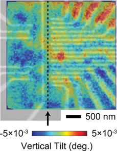
Increasing the number of quantum bits while preserving precise control of their quantum electronic properties is a significant challenge in materials design for the development of semiconductor quantum computing devices. Semiconductor heterostructures can host multiple quantum dots that are electrostatically defined by voltages applied to an array of metallic nanoelectrodes. The structural distortion of multiple-quantum-dot devices due to elastic stress associated with the electrodes has been difficult to predict because of the large micrometer-scale overall sizes of the devices, the complex spatial arrangement of the electrodes, and the sensitive dependence of the magnitude and spatial variation of the stress on processing conditions. Synchrotron X-ray nanobeam Bragg diffraction studies of a GaAs/AlGaAs heterostructure reveal the magnitude and nanoscale variation of these distortions. Investigations of individual linear electrodes reveal lattice tilts consistent with a 28-MPa compressive residual stress in the electrodes. The angular magnitude of the tilts varies by up to 20% over distances of less than 200 nm along the length of the electrodes, consistent with heterogeneity in the metal residual stress. A similar variation of the crystal tilt is observed in multiple-quantum-dot devices, due to a combination of the variation of the stress and the complex electrode arrangement. The heterogeneity in particular can lead to significant challenges in the scaling of multiple-quantum-dot devices due to differences between the charging energies of dots and uncertainty in the potential energy landscape. Alternatively, if incorporated in design, stress presents a new degree of freedom in device fabrication.

Type
Invited Paper
Copyright
Copyright © Materials Research Society 2019 

Access options

Get access to the full version of this content by using one of the access options below. (Log in options will check for institutional or personal access. Content may require purchase if you do not have access.)

References

Zwanenburg, F.A., Dzurak, A.S., Morello, A., Simmons, M.Y., Hollenberg, L.C.L., Klimeck, G., Rogge, S., Coppersmith, S.N., and Eriksson, M.A.: Silicon quantum electronics. Rev. Mod. Phys. 85, 961 (2013).CrossRefGoogle Scholar
Vandersypen, L.M.K., Steffen, M., Breyta, G., Yannoni, C.S., Sherwood, M.H., and Chuang, I.L.: Experimental realization of Shor’s quantum factoring algorithm using nuclear magnetic resonance. Nature 414, 883 (2001).CrossRefGoogle ScholarPubMed
Bernien, H., Schwartz, S., Keesling, A., Levine, H., Omran, A., Pichler, H., Choi, S., and Zibrov, A.S.: Probing many-body dynamics on a 51-atom quantum simulator. Nature 551, 579 (2017).CrossRefGoogle ScholarPubMed
Zhang, J., Pagano, G., Hess, P.W., Kyprianidis, A., Becker, P., Kaplan, H., Gorshkov, A.V., Gong, Z.X., and Monroe, C.: Observation of a many-body dynamical phase transition with a 53-qubit quantum simulator. Nature 551, 601 (2017).CrossRefGoogle ScholarPubMed
Hanson, R., Kouwenhoven, L.P., Petta, J.R., Tarucha, S., and Vandersypen, L.M.K.: Spins in few-electron quantum dots. Rev. Mod. Phys. 79, 1217 (2007).CrossRefGoogle Scholar
Hastings, M.B., Wecker, D., Bauer, B., and Troyer, M.: Improving quantum algorithms for quantum chemistry. Quantum Inf. Comput. 15, 1 (2015).Google Scholar
Vandersypen, L.M.K., Bluhm, H., Clarke, J.S., Dzurak, A.S., Ishihara, R., Morello, A., Reilly, D.J., Schreiber, L.R., and Veldhorst, M.: Interfacing spin qubits in quantum dots and donors-hot, dense, and coherent. npj Quant. Inf. 3, 34 (2017).CrossRefGoogle Scholar
Landig, A.J., Koski, J.V., Scarlino, P., Mendes, U.C., Blais, A., Reichl, C., Wegscheider, W., Wallraff, A., Ensslin, K., and Ihn, T.: Coherent spin-photon coupling using a resonant exchange qubit. Nature 560, 179 (2018).CrossRefGoogle ScholarPubMed
Samkharadze, N., Zheng, G., Kalhor, N., Brousse, D., Sammak, A., Mendes, U.C., Blais, A., Scappucci, G., and Vandersypen, L.M.K.: Strong spin-photon coupling in silicon. Science 359, 1123 (2018).CrossRefGoogle ScholarPubMed
Mi, X., Benito, M., Putz, S., Zajac, D.M., Taylor, J.M., Burkard, G., and Petta, J.R.: A coherent spin–photon interface in silicon. Nature 555, 599 (2018).CrossRefGoogle ScholarPubMed
Ito, T., Otsuka, T., Amaha, S., Delbecq, M.R., Nakajima, T., Yoneda, J., Takeda, K., Allison, G., Noiri, A., Kawasaki, K., and Tarucha, S.: Detection and control of charge states in a quintuple quantum dot. Sci. Rep. 6, 39113 (2016).CrossRefGoogle Scholar
Park, J., Ahn, Y., Tilka, J.A., Sampson, K.C., Savage, D.E., Prance, J.R., Simmons, C.B., Lagally, M.G., Coppersmith, S.N., Eriksson, M.A., Holt, M.V., and Evans, P.G.: Electrode-stress-induced nanoscale disorder in Si quantum electronic devices. APL Mater. 4, 0661021 (2016).CrossRefGoogle Scholar
Pateras, A., Park, J., Ahn, Y., Tilka, J.A., Holt, M.V., Reichl, C., Wegscheider, W., Baart, T.A., Dehollain, J-P., Mukhopadhyay, U., Vandersypen, L.M.K., and Evans, P.G.: Mesoscopic elastic distortions in GaAs quantum dot heterostructures. Nano Lett. 18, 2780 (2018).CrossRefGoogle ScholarPubMed
Davies, J.H. and Larkin, I.A.: Theory of potential modulation in lateral surface superlattices. Phys. Rev. B 49, 4800 (1994).CrossRefGoogle ScholarPubMed
Larkin, I.A., Davies, J.H., Long, A.R., and Cuscó, R.: Theory of potential modulation in lateral surface superlattices. II. Piezoelectric effect. Phys. Rev. B 56, 15242 (1997).CrossRefGoogle Scholar
Chaudhari, P.: Grain growth and stress relief in thin films. J. Vac. Sci. Technol. 9, 520 (1972).CrossRefGoogle Scholar
Hytch, M.J. and Minor, A.M.: Observing and measuring strain in nanostructures and devices with transmission electron microscopy. MRS Bull. 39, 138 (2014).CrossRefGoogle Scholar
Hytch, M.J., Putaux, J.L., and Penisson, J.M.: Measurement of the displacement field of dislocations to 0.03 angstrom by electron microscopy. Nature 423, 270 (2003).CrossRefGoogle Scholar
Durbin, S.M. and Follis, G.C.: Darwin theory of heterostructure diffraction. Phys. Rev. B 51, 10127 (1995).CrossRefGoogle ScholarPubMed
Pateras, A., Park, J., Ahn, Y., Holt, M.V., Kim, H., Mawst, L.J., and Evans, P.G.: Dynamical scattering in coherent hard X-ray nanobeam Bragg diffraction. Phys. Rev. B 97, 235414 (2018).CrossRefGoogle Scholar
Tilka, J.A., Park, J., Ahn, Y., Pateras, A., Sampson, K.C., Savage, D.E., Prance, J.R., Simmons, C.B., Coppersmith, S.N., Eriksson, M.A., Lagally, M.G., Holt, M.V., and Evans, P.G.: Combining experiment and optical simulation in coherent X-ray nanobeam characterization of Si/SiGe semiconductor heterostructures. J. Appl. Phys. 120, 015304 (2016).CrossRefGoogle Scholar
Blech, I.A. and Meieran, E.S.: Enhanced X-ray diffraction from substrate crystals containing discontinuous surface films. J. Appl. Phys. 38, 2913 (1967).CrossRefGoogle Scholar
Gehrsitz, S., Sigg, H., Herres, N., Bachem, K., Kohler, K., and Reinhart, F.K.: Compositional dependence of the elastic constants and the lattice parameter of AlxGa1−xAs. Phys. Rev. B 60, 11601 (1999).CrossRefGoogle Scholar
Chason, E., Sheldon, B.W., Freund, L.B., Floro, J.A., and Hearne, S.J.: Origin of compressive residual stress in polycrystalline thin films. Phys. Rev. Lett. 88, 689 (2002).CrossRefGoogle ScholarPubMed
Floro, J.A., Hearne, S.J., Hunter, J.A., Kotula, P., Chason, E., Seel, S.C., and Thompson, C.V.: The dynamic competition between stress generation and relaxation mechanisms during coalescence of Volmer–Weber thin films. J. Appl. Phys. 89, 4886 (2001).CrossRefGoogle Scholar
Nix, W.D. and Clemens, B.M.: Crystallite coalescence: A mechanism for intrinsic tensile stresses in thin films. J. Mater. Res. 14, 3467 (1999).CrossRefGoogle Scholar
Freund, L.B. and Suresh, S.: Thin Film Materials: Stress, Defect Formation and Surface Evolution (Cambridge University Press, U.K., 2003).Google Scholar
Flinn, P.A., Gardner, D.S., and Nix, W.D.: Measurement and interpretation of stress in aluminum-based metallization as a function of thermal history. IEEE Trans. Electron Devices 34, 689 (1987).CrossRefGoogle Scholar
Hodge, T.C., Bidstrup-Allen, S.A., and Kohl, P.A.: Stresses in thin film metallization. IEEE Trans. Compon., Packag., Manuf. Technol., Part A 20, 241 (1997).CrossRefGoogle Scholar
Dong, M., Cui, X., Wang, H., Zhu, L., Jin, G., and Xu, B.: Effect of different substrate temperatures on microstructure and residual stress of Ti films. Rare Met. Mater. Eng. 45, 843 (2016).CrossRefGoogle Scholar
Zhou, S., Wu, W., and Shao, T.: Effect of post deposition annealing on residual stress stability of gold films. Surf. Coat. Technol. 304, 222 (2016).CrossRefGoogle Scholar
Thorbeck, T. and Zimmerman, N.M.: Formation of strain-induced quantum dots in gated semiconductor nanostructures. AIP Adv. 5, 087107 (2015).CrossRefGoogle Scholar
Skuras, E., Long, A.R., Larkin, I.A., Davies, J.H., and Holland, M.C.: Anisotropic piezoelectric effect in lateral surface superlattices. Appl. Phys. Lett. 70, 871 (1997).CrossRefGoogle Scholar
Fischer, J., Trif, M., Coish, W.A., and Loss, D.: Spin interactions, relaxation and decoherence in quantum dots. Solid State Commun. 149, 1443 (2009).CrossRefGoogle Scholar
Shabalin, A.G., Yefanov, O.M., Nosik, V.L., Bushuev, V.A., and Vartanyants, I.A.: Dynamical effects in Bragg coherent X-ray diffraction imaging of finite crystals. Phys. Rev. B 96, 064111 (2017).CrossRefGoogle Scholar
Ying, A., Osting, B., Noyan, I.C., Murray, C.E., Holt, M., and Maser, J.: Modeling of kinematic diffraction from a thin silicon film illuminated by a coherent, focused X-ray nanobeam. J. Appl. Crystallogr. 43, 587 (2010).CrossRefGoogle Scholar
Hönig, S., Hoppe, R., Patommel, J., Schropp, A., Stephan, S., Schöder, S., Burghammer, M., and Schroer, C.G.: Full optical characterization of coherent X-ray nanobeams by ptychographic imaging. Opt. Express 19, 16324 (2011).CrossRefGoogle ScholarPubMed
Goodman, J.: Introduction to Fourier Optics (McGraw-Hill, New York, 1996).Google Scholar