Hostname: page-component-78c5997874-lj6df Total loading time: 0 Render date: 2024-11-04T21:28:03.316Z Has data issue: false hasContentIssue false

Effects of buffer layer thickness on the surface roughness of In0.3Ga0.7As thin films: A phase-field simulation

Published online by Cambridge University Press:  19 November 2013

Pingping Wu
Affiliation:
State Key Laboratory of Luminescent Materials and Devices, South China University of Technology, Guangzhou 510641, China
Fangliang Gao
Affiliation:
State Key Laboratory of Luminescent Materials and Devices, South China University of Technology, Guangzhou 510641, China
Guoqiang Li*
Affiliation:
State Key Laboratory of Luminescent Materials and Devices, South China University of Technology, Guangzhou 510641, China
*
a)Address all correspondence to this author. e-mail: [email protected]
Get access

Abstract

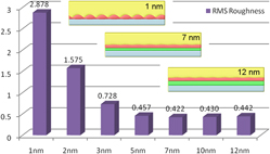
The graded composition buffer layers are very commonly used in the semiconductor triple-junction solar cell device. To grow a strain-free 1.0-eV In0.3Ga0.7As thin film on a GaAs substrate, a total of 2.2% misfit strain must be relaxed through well-designed buffer layer structures. In this work, a phase-field model of a multilayered system is developed to probe the roughness of top surface morphology and predict optimal buffer layer thickness. Our simulation shows time evolution of the thin film morphology and the root-mean-square roughness of the surface with different buffer layer thickness designs. The strain distribution is investigated to explain the surface morphology evolution with the effect of the buffer layer. The simulation results show that the buffer layer thickness is a key parameter that affects the quality of the In0.3Ga0.7As epilayers. The simulation results can be effective in improving the design of graded buffer layers.

Type
Articles
Copyright
Copyright © Materials Research Society 2013 

Access options

Get access to the full version of this content by using one of the access options below. (Log in options will check for institutional or personal access. Content may require purchase if you do not have access.)

References

REFERENCES

King, R.R., Law, D.C., Edmondson, K.M., Fetzer, C.M., Kinsey, G.S., Yoon, H., Sherif, R.A., and Karam, N.H.: 40% efficient metamorphic GaInP/GaInAs/Ge multijunction solar cells. Appl. Phys. Lett. 90, 183516 (2007).CrossRefGoogle Scholar
Guter, W., Schöne, J., Philipps, S.P., Steiner, M., Siefer, G., Wekkeli, A., Welser, E., Oliva, E., Bett, A.W., and Dimroth, F.: Current-matched triple-junction solar cell reaching 41.1% conversion efficiency under concentrated sunlight. Appl. Phys. Lett. 94, 223504 (2009).CrossRefGoogle Scholar
Wiemer, M., Sabnis, V., and Yuen, H.: 43.5% efficient lattice matched solar cells. Proc. SPIE, Vol. 8108, 810804, High and Low Concentrator Systems for Solar Electric Applications VI (2011). doi: 10.1117/12.897769.Google Scholar
Luque, A.: Will we exceed 50% efficiency in photovoltaics? J. Appl. Phys. 110, 031301 (2011).CrossRefGoogle Scholar
Dunstan, D.J.: Relaxed buffer layers. Semicond. Sci. Technol. 6, A76 (1991).CrossRefGoogle Scholar
Zhang, J.C., Zhao, D.G., Wang, J.F., Wang, Y.T., Chen, J., Liu, J.P., and Yang, H.: The influence of AlN buffer layer thickness on the properties of GaN epilayer. J. Cryst. Growth 268, 24 (2004).CrossRefGoogle Scholar
Wang, X.L., Zhao, D.G., Li, X.Y., Gong, H.M., Yang, H., and Liang, J.W.: The effects of LT AlN buffer thickness on the properties of high Al composition AlGaN epilayers. Mater. Lett. 60, 3693 (2006).CrossRefGoogle Scholar
Luo, W.J., Wang, X.L., Guo, L.C., Xiao, H.L., Wang, C.M., Ran, J.X., Li, J.P., and Li, J.M.: Influence of AlN buffer layer thickness on the properties of GaN epilayer on Si(1 1 1) by MOCVD. Microelectron. J. 39 1710 (2008).CrossRefGoogle Scholar
Nakamura, S.: GaN growth using GaN buffer layer. J. Appl. Phys. 30, L1705 (1991).CrossRefGoogle Scholar
Gonzalez, L., García, J.M., García, R., Briones, F., Martínez-Pastor, J., and Ballesteros, C.: Influence of buffer-layer surface morphology on the self-organized growth of InAs on InP(001) nanostructures. Appl. Phys. Lett. 76, 1104 (2000).CrossRefGoogle Scholar
Piquette, E.C., Bridger, P.M., Beach, R.A., and McGill, T.C.: Effect of buffer layer and III/V ratio on the surface morphology of Gan grown by MBE. In MRS Proceedings, Vol. 537, 1998; p. G3.77. doi:10.1557/PROC-537–G3.77.Google Scholar
Asaro, R.J. and Tiller, W.A.: Interface morphology development during stress corrosion cracking: Part I. Via surface diffusion. Metall. Trans. 3, 1789 (1972).CrossRefGoogle Scholar
Grinfeld, M.A.: Instability of the separation boundry between a nonhydrostatically stressed elastic body and a melt. Sov. Phys. Dokl. 31, 831 (1986).Google Scholar
Srolovitz, D.J.: On the stability of surfaces of stressed solids. Acta Metall. 37, 621 (1989).CrossRefGoogle Scholar
Gao, H.: Some general properties of stress-driven surface evolution in a heteroepitaxial thin film structure. J. Mech. Phys. Solids 42, 741 (1994).CrossRefGoogle Scholar
Tersoff, J. and LeGoues, F.K.: Competing relaxation mechanisms in strained layers. Phys. Rev. Lett. 72, 3570 (1994).CrossRefGoogle ScholarPubMed
Krishnamurthy, R. and Srolovitz, D.J.: Film/substrate interface stability in thin films. J. Appl. Phys. 99, 043504 (2006).CrossRefGoogle Scholar
Lu, G.H. and Liu, F.: Towards quantitative understanding of formation and stability of Ge hut islands on Si(001). Phys. Rev. Lett. 94, 176103 (2005).CrossRefGoogle ScholarPubMed
Liu, F.: Self-assembly of three-dimensional metal islands: Nonstrained versus strained islands. Phys. Rev. Lett. 89, 246105 (2002).CrossRefGoogle ScholarPubMed
Wang, H., Zhang, Y., and Liu, F.: Enhanced growth instability of strained film on wavy substrate. J. Appl. Phys. 104, 054301 (2008).CrossRefGoogle Scholar
Hu, H., Gao, H.J., and Liu, F.: Theory of directed nucleation of strained islands on patterned substrates. Phys. Rev. Lett. 101, 216102 (2008).CrossRefGoogle ScholarPubMed
Wang, Y.U., Jin, Y.M., and Khachaturyan, A.G.: Phase field microelasticity modeling of surface instability of heteroepitaxial thin films. Acta. Mater. 52, 81 (2004).CrossRefGoogle Scholar
Seol, D.J., Hu, S.Y., Liu, Z.K., Chen, L.Q., Kim, S.G., and Oh, K.H.: Phase-field modeling of stress-induced surface instabilities in heteroepitaxial thin films. J. Appl. Phys. 98, 044910 (2005).CrossRefGoogle Scholar
Ni, Y., He, L.H., and Soh, A.K.: Three-dimensional phase field simulation for surface roughening of heteroepitaxial films with elastic anisotropy. J. Cryst. Growth 284, 281 (2005).CrossRefGoogle Scholar
Takaki, T., Hirouchi, T., and Tomita, Y.: Phase-field study of interface energy effect on quantum dot morphology. J. Cryst. Growth 310, 2248 (2008).CrossRefGoogle Scholar
Kurtz, S.R., Myers, D., and Olson, J.M.: Projected performance of three- and four-junction devices using GaAs and GaInP. In Photovoltaic Specialists Conference, 1997; Conference Record of the Twenty-Sixth IEEE, 1997; pp. 875–878. doi: 10.1109/PVSC.1997.654226. Google Scholar
Friedman, D.J., Geisz, J.F., Norman, A.G., Wanlass, M.W., and Kurtz, S.R.: 0.7-eV GaInAs junction for a GaInP/GaAs/GaInAs(1eV)/GaInAs(0.7eV) four-junction solar cell. 4th World Conference on Photovoltaic Energy Conversion, 2006; p. 598602. doi: 10.1109/WCPEC.2006.279527.Google Scholar
Geisz, J.F., Kurtz, S.R., Wanlass, M.W., Ward, J.S., Duda, A., Friedman, D.J., Olson, J.M., McMahon, W.E., Moriarty, T.E., Kiehl, J.T., Romero, M.J., Norman, A.G., and Jone, K.M.: Inverted GaInP/(In)GaAs/InGaAs triple-junction solar cells with low-stress metamorphic bottom junctions. In Photovoltaic Specialists Conference San Diego, California May 11–16, 2008, 33rd IEEE; 2008; pp. 15. doi: 10.1109/PVSC.2008.4922452.CrossRefGoogle Scholar
Sze, S.M.: Physics of Semiconductor Devices, 2nd ed. (Wiley, New York, 1981).Google Scholar
Pillai, M.R., Kim, S-S., Ho, S.T., and Barnett, S.A.: Growth of In x Ga1−x As/GaAs heterostructures using Bi as a surfactant. J. Vac. Sci. Technol., B 18, 1232 (2000).CrossRefGoogle Scholar
Matthews, J.W. and Blakeslee, A.E.: Defects in epitaxial multilayers: III. Preparation of almost perfect multilayers. J. Cryst. Growth 32, 265 (1976).CrossRefGoogle Scholar
Millunchick, J.M. and Barnett, S.A.: Suppression of strain relaxation and roughening of InGaAs on GaAs using ion-assisted molecular beam epitaxy. Appl. Phys. Lett. 65, 1136 (1994).CrossRefGoogle Scholar
Khachaturyan, A.G.: Theory of Structural Transformations in Solids (Wiley, New York, 1983).Google Scholar
Chen, L.Q. and Shen, J.: Applications of semi-implicit Fourier-spectral method to phase field equations. Comput. Phys. Commun. 108, 147 (1998).CrossRefGoogle Scholar
Kurilo, I.V. and Guba, S.K.: Misfit dislocations and stress in In1-xGaxAs/GaAs heterostructures. Inorg. Mater. 47, 819 (2011).CrossRefGoogle Scholar
Anan, T., Nishi, K., and Sugou, S.: Critical layer thickness on (111)B‐oriented InGaAs/GaAs heteroepitaxy. Appl. Phys. Lett. 60, 3159 (1992).CrossRefGoogle Scholar
Chuang, S.L.: Physics of Optoelectronic Devices (Wiley, New York, 1995).Google Scholar
Mariager, S.O., Lauridsen, S.L., Dohn, A., Bovet, N., Sørensen, C.B., Schleputz, C.M., Willmott, P.R., and Feidenhans'l, R.: High-resolution three-dimensional reciprocal-space mapping of InAs nanowires. J. Appl. Cryst. 42 369, (2009).CrossRefGoogle Scholar
Pelliccione, M. and Lu, T.M.: Evolution of Thin Film Morphology Modeling and Simulations (Springer, New York, 2007).Google Scholar
Matthews, J.W. and Blakeslee, A.E.: Defects in epitaxial multilayers: I. Misfit dislocations. J. Cryst. Growth 27, 118 (1974).Google Scholar
Bertolet, D.C., Hsu, J-K., Agahi, F., and Lau, K.M.: Critical thickness of GaAs/InGaAs and AlGaAs/GaAsP strained quantum wells grown by organometallic chemical vapor deposition. J. Electron. Mater. 19, 967 (1990).CrossRefGoogle Scholar
Krieger, M., Sigg, H., Herres, N., Bachem, K., and Kohler, K.: Elastic constants and Poisson ratio in the system AlAs–GaAs. Appl. Phys. Lett. 66, 682 (1994).CrossRefGoogle Scholar
Hoke, W.E., Kennedy, T.D., and Torabi, A.: Simultaneous determination of Poisson ratio, bulk lattice constant, and composition of ternary compounds In0.3Ga0.7As, In0.3Al0.7As, In0.7Ga0.3P, and In0.7Al0.3P. Appl. Phys. Lett. 79, 4160 (2001).CrossRefGoogle Scholar
Orders, P.J. and Usher, B.F.: Determination of critical layer thickness in In x Ga1−x As/GaAs heterostructures by x-ray diffraction. Appl. Phys. Lett. 50, 980 (1987).CrossRefGoogle Scholar
Jasik, A., Sass, J., Mazur, K., and Wesolowski, M.: Investigation of strained InGaAs layers on GaAs substrate. Opt. Appl. 37, 237 (2007).Google Scholar
Zhang, X., Briot, O., Gil, B., and Aulombard, R.: Critical layer thickness in MOCVD grown InGaAs/GaAs strained quantum wells. Mater. Sci. Eng., B 35, 184 (1995).CrossRefGoogle Scholar