Hostname: page-component-78c5997874-dh8gc Total loading time: 0 Render date: 2024-11-04T21:07:04.992Z Has data issue: false hasContentIssue false

Distinct photoluminescence and Raman spectroscopy signatures for identifying highly crystalline WS2 monolayers produced by different growth methods

Published online by Cambridge University Press:  08 March 2016

Amber McCreary
Affiliation:
Department of Physics and Center for 2-Dimensional and Layered Materials, The Pennsylvania State University, University Park, Pennsylvania 16802, USA
Ayse Berkdemir
Affiliation:
Department of Physics and Center for 2-Dimensional and Layered Materials, The Pennsylvania State University, University Park, Pennsylvania 16802, USA; and Nanotechnology Research Center and Kayseri Vocational College, Erciyes University, Kayseri 38039, Turkey
Junjie Wang
Affiliation:
Department of Physics and Center for 2-Dimensional and Layered Materials, The Pennsylvania State University, University Park, Pennsylvania 16802, USA
Minh An Nguyen
Affiliation:
Department of Chemistry, The Pennsylvania State University, University Park, Pennsylvania 16802, USA
Ana Laura Elías
Affiliation:
Department of Physics and Center for 2-Dimensional and Layered Materials, The Pennsylvania State University, University Park, Pennsylvania 16802, USA
Néstor Perea-López
Affiliation:
Department of Physics and Center for 2-Dimensional and Layered Materials, The Pennsylvania State University, University Park, Pennsylvania 16802, USA
Kazunori Fujisawa
Affiliation:
Department of Physics and Center for 2-Dimensional and Layered Materials, The Pennsylvania State University, University Park, Pennsylvania 16802, USA
Bernd Kabius
Affiliation:
Materials Research Institute, The Pennsylvania State University, University Park, Pennsylvania 16802, USA
Victor Carozo
Affiliation:
Department of Physics and Center for 2-Dimensional and Layered Materials, The Pennsylvania State University, University Park, Pennsylvania 16802, USA
David A. Cullen
Affiliation:
Materials Science & Technology Division, Oak Ridge National Laboratory, Oak Ridge, TN 37831, USA
Thomas E. Mallouk
Affiliation:
Department of Chemistry, The Pennsylvania State University, University Park, Pennsylvania 16802, USA
J. Zhu
Affiliation:
Department of Physics and Center for 2-Dimensional and Layered Materials, The Pennsylvania State University, University Park, Pennsylvania 16802, USA
Mauricio Terrones*
Affiliation:
Department of Physics and Center for 2-Dimensional and Layered Materials, The Pennsylvania State University, University Park, Pennsylvania 16802, USA; Department of Chemistry, The Pennsylvania State University, University Park, Pennsylvania 16802, USA; Department of Materials Science & Engineering, The Pennsylvania State University, University Park, Pennsylvania 16802, USA; and Research Center for Exotic Nanocarbons, Shinshu University, Nagano 380-8553, Japan
*
a) Address all correspondence to this author. e-mail: [email protected]
Get access

Abstract

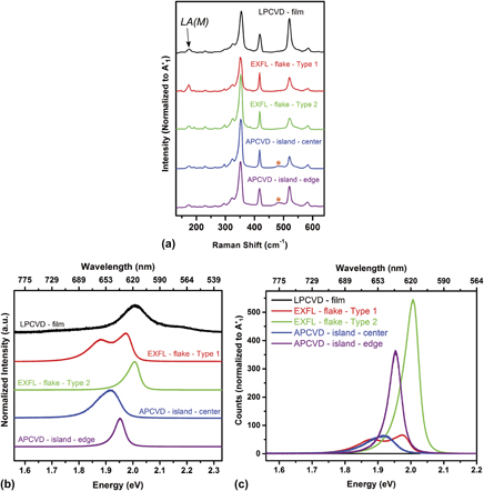
Transition metal dichalcogenides such as WS2 show exciting promise in electronic and optoelectronic applications. Significant variations in the transport, Raman, and photoluminescence (PL) can be found in the literature, yet it is rarely addressed why this is. In this report, Raman and PL of monolayered WS2 produced via different methods are studied and distinct features that indicate the degree of crystallinity of the material are observed. While the intensity of the LA(M) Raman mode is found to be a useful indicator to assess the crystallinity, PL is drastically more sensitive to the quality of the material than Raman spectroscopy. We also show that even exfoliated crystals, which are usually regarded as the most pristine material, can contain large amounts of defects that would not be apparent without Raman and PL measurements. These findings can be applied to the understanding of other two-dimensional heterostructured systems.

Type
Invited Articles
Copyright
Copyright © Materials Research Society 2016 

Access options

Get access to the full version of this content by using one of the access options below. (Log in options will check for institutional or personal access. Content may require purchase if you do not have access.)

References

REFERENCES

Geim, A.K. and Novoselov, K.S.: The rise of graphene. Nat. Mater. 6(3), 183 (2007).CrossRefGoogle ScholarPubMed
Kim, K.K., Hsu, A., Jia, X., Kim, S.M., Shi, Y., Dresselhaus, M., Palacios, T., and Kong, J.: Synthesis and characterization of hexagonal boron nitride film as a dielectric layer for graphene devices. ACS Nano 6(10), 8583 (2012).Google Scholar
Dean, C.R., Young, A.F., Meric, I., Lee, C., Wang, L., Sorgenfrei, S., Watanabe, K., Taniguchi, T., Kim, P., Shepard, K.L., and Hone, J.: Boron nitride substrates for high-quality graphene electronics. Nat. Nanotechnol. 5(10), 722 (2010).Google Scholar
Novoselov, K.S. and Castro Neto, A.H.: Two-dimensional crystals-based heterostructures: Materials with tailored properties. Phys. Scr. T146, 014006 (2012).Google Scholar
Wang, Q.H., Kalantar-Zadeh, K., Kis, A., Coleman, J.N., and Strano, M.S.: Electronics and optoelectronics of two-dimensional transition metal dichalcogenides. Nat. Nanotechnol. 7(11), 699 (2012).Google Scholar
Berkdemir, A., Gutierrez, H.R., Botello-Mendez, A.R., Perea-Lopez, N., Elias, A.L., Chia, C-I., Wang, B., Crespi, V.H., Lopez-Urias, F., Charlier, J-C., Terrones, H., and Terrones, M.: Identification of individual and few layers of WS2 using Raman spectroscopy. Sci. Rep. 3, 1755 (2013).CrossRefGoogle Scholar
Chhowalla, M., Shin, H.S., Eda, G., Li, L.J., Loh, K.P., and Zhang, H.: The chemistry of two-dimensional layered transition metal dichalcogenide nanosheets. Nat. Chem. 5(4), 263 (2013).CrossRefGoogle ScholarPubMed
Mak, K.F., Lee, C., Hone, J., Shan, J., and Heinz, T.F.: Atomically thin MoS2: A new direct-gap semiconductor. Phys. Rev. Lett. 105(13), 136805 (2010).Google Scholar
Lopez-Sanchez, O., Lembke, D., Kayci, M., Radenovic, A., and Kis, A.: Ultrasensitive photodetectors based on monolayer MoS2 . Nat. Nanotechnol. 8(7), 497 (2013).Google Scholar
Butler, S.Z., Hollen, S.M., Cao, L., Cui, Y., Gupta, J.A., Gutierrez, H.R., Heinz, T.F., Hong, S.S., Huang, J., Ismach, A.F., Johnston-Halperin, E., Kuno, M., Plashnitsa, V.V., Robinson, R.D., Ruoff, R.S., Salahuddin, S., Shan, J., Shi, L., Spencer, M.G., Terrones, M., Windl, W., and Goldberger, J.E.: Progress, challenges, and opportunities in two-dimensional materials beyond graphene. ACS Nano 7(4), 2898 (2013).Google Scholar
Jariwala, D., Sangwan, V.K., Lauhon, L.J., Marks, T.J., and Hersam, M.C.: Emerging device applications for semiconducting two-dimensional transition metal dichalcogenides. ACS Nano 8(2), 1102 (2014).Google Scholar
Ganatra, R. and Zhang, Q.: Few-layer MoS2: A promising layered semiconductor. ACS Nano 8(5), 4074 (2014).CrossRefGoogle ScholarPubMed
Gutierrez, H.R., Perea-Lopez, N., Elias, A.L., Berkdemir, A., Wang, B., Lv, R., Lopez-Urias, F., Crespi, V.H., Terrones, H., and Terrones, M.: Extraordinary room-temperature photoluminescence in triangular WS2 monolayers. Nano Lett. 13(8), 3447 (2013).CrossRefGoogle ScholarPubMed
Elias, A.L., Perea-Lopez, N., Castro-Beltran, A., Berkdemir, A., Lv, R.T., Feng, S.M., Long, A.D., Hayashi, T., Kim, Y.A., Endo, M., Gutierrez, H.R., Pradhan, N.R., Balicas, L., Houk, T.E.M., Lopez-Urias, F., Terrones, H., and Terrones, M.: Controlled synthesis and transfer of large-area WS2 sheets: From single layer to few layers. ACS Nano 7(6), 5235 (2013).CrossRefGoogle ScholarPubMed
Orofeo, C.M., Suzuki, S., Sekine, Y., and Hibino, H.: Scalable synthesis of layer-controlled WS2 and MoS2 sheets by sulfurization of thin metal films. Appl. Phys. Lett. 105(8), 83112 (2014).Google Scholar
Jo, S., Ubrig, N., Berger, H., Kuzmenko, A.B., and Morpurgo, A.F.: Mono- and bilayer WS2 light-emitting transistors. Nano Lett. 14(4), 2019 (2014).CrossRefGoogle ScholarPubMed
Zhang, Y., Zhang, Y., Ji, Q., Ju, J., Yuan, H., Shi, J., Gao, T., Ma, D., Liu, M., Chen, Y., Song, X., Hwang, H.Y., Cui, Y., and Liu, Z.: Controlled growth of high-quality monolayer WS2 layers on sapphire and imaging its grain boundary. ACS Nano 7(10), 8963 (2013).Google Scholar
Rong, Y., Fan, Y., Leen Koh, A., Robertson, A.W., He, K., Wang, S., Tan, H., Sinclair, R., and Warner, J.H.: Controlling sulphur precursor addition for large single crystal domains of WS2 . Nanoscale 6(20), 12096 (2014).CrossRefGoogle ScholarPubMed
Zhao, W., Ghorannevis, Z., Chu, L., Toh, M., Kloc, C., Tan, P-H., and Eda, G.: Evolution of electronic structure in atomically thin sheets of WS2 and WSe2 . ACS Nano 7(1), 791 (2013).Google Scholar
Mitioglu, A.A., Plochocka, P., Jadczak, J.N., Escoffier, W., Rikken, G.L.J.A., Kulyuk, L., and Maude, D.K.: Optical manipulation of the exciton charge state in single-layer tungsten disulfide. Phys. Rev. B 88(24), 245403 (2013).Google Scholar
Zeng, H.L., Liu, G.B., Dai, J.F., Yan, Y.J., Zhu, B.R., He, R.C., Xie, L., Xu, S.J., Chen, X.H., Yao, W., and Cui, X.D.: Optical signature of symmetry variations and spin-valley coupling in atomically thin tungsten dichalcogenides. Sci. Rep. 3, 1608 (2013).Google Scholar
Novoselov, K.S., Jiang, D., Schedin, F., Booth, T.J., Khotkevich, V.V., Morozov, S.V., and Geim, A.K.: Two-dimensional atomic crystals. Proc. Natl. Acad. Sci. U. S. A. 102(30), 10451 (2005).Google Scholar
Eda, G., Yamaguchi, H., Voiry, D., Fujita, T., Chen, M.W., and Chhowalla, M.: Photoluminescence from chemically exfoliated MoS2 . Nano Lett. 11(12), 5111 (2011).Google Scholar
Coleman, J.N., Lotya, M., O'Neill, A., Bergin, S.D., King, P.J., Khan, U., Young, K., Gaucher, A., De, S., Smith, R.J., Shvets, I.V., Arora, S.K., Stanton, G., Kim, H-Y., Lee, K., Kim, G.T., Duesberg, G.S., Hallam, T., Boland, J.J., Wang, J.J., Donegan, J.F., Grunlan, J.C., Moriarty, G., Shmeliov, A., Nicholls, R.J., Perkins, J.M., Grieveson, E.M., Theuwissen, K., McComb, D.W., Nellist, P.D., and Nicolosi, V.: Two-dimensional nanosheets produced by liquid exfoliation of layered materials. Science 331(6017), 568 (2011).Google Scholar
Matte, H.S.S.R., Gomathi, A., Manna, A.K., Late, D.J., Datta, R., Pati, S.K., and Rao, C.N.R.: MoS2 and WS2 analogues of graphene. Angew. Chem., Int. Ed. 49(24), 4059 (2010).Google Scholar
Frindt, R.F.: Single crystals of MoS2 several molecular layers thick. J. Appl. Phys. 37(4), 1928 (1966).CrossRefGoogle Scholar
Joensen, P., Frindt, R.F., and Morrison, S.R.: Single layer MoS2 . Mater. Res. Bull. 21(4), 457 (1986).Google Scholar
Golasa, K., Grzeszczyk, M., Korona, K.P., Bozek, R., Binder, J., Szczytko, J., Wysmolek, A., and Babinski, A.: Optical properties of molybdenum disulfide (MoS2). Acta Phys. Pol., A 124(5), 849 (2013).Google Scholar
Schäfer, H., Grofe, T., and Trenkel, M.: The chemical transport of molybdenum and tungsten and of their dioxides and sulfides. J. Solid State Chem. 8(1), 14 (1973).Google Scholar
Lieth, R.M.A.: Preparation and Crystal Growth of Materials with Layered Structures, Vol. 1 (D. Reidel Pub. Co, Dordrecht, 1977).CrossRefGoogle Scholar
Nicolosi, V., Chhowalla, M., Kanatzidis, M.G., Strano, M.S., and Coleman, J.N.: Liquid exfoliation of layered materials. Science 340(6139), 1420 (2013).Google Scholar
Dresselhaus, M.S. and Dresselhaus, G.: Intercalation compounds of graphite. Adv. Phys. 30(2), 139 (1981).Google Scholar
van der Zande, A.M., Huang, P.Y., Chenet, D.A., Berkelbach, T.C., You, Y.M., Lee, G.H., Heinz, T.F., Reichman, D.R., Muller, D.A., and Hone, J.C.: Grains and grain boundaries in highly crystalline monolayer molybdenum disulphide. Nat. Mater. 12(6), 554 (2013).Google Scholar
Shaw, J.C., Zhou, H., Chen, Y., Weiss, N.O., Liu, Y., Huang, Y., and Duan, X.: Chemical vapor deposition growth of monolayer MoSe2 nanosheets. Nano Res. 7(4), 511 (2014).CrossRefGoogle Scholar
Kang, K., Xie, S., Huang, L., Han, Y., Huang, P.Y., Mak, K.F., Kim, C-J., Muller, D., and Park, J.: High-mobility three-atom-thick semiconducting films with wafer-scale homogeneity. Nature 520(7549), 656 (2015).Google Scholar
Splendiani, A., Sun, L., Zhang, Y.B., Li, T.S., Kim, J., Chim, C.Y., Galli, G., and Wang, F.: Emerging photoluminescence in monolayer MoS2 . Nano Lett. 10(4), 1271 (2010).Google Scholar
Baugher, B.W.H., Churchill, H.O.H., Yang, Y., and Jarillo-Herrero, P.: Intrinsic electronic transport properties of high-quality monolayer and bilayer MoS2 . Nano Lett. 13(9), 4212 (2013).Google Scholar
Fang, H., Chuang, S., Chang, T.C., Takei, K., Takahashi, T., and Javey, A.: High-performance single layered WSe2 p-FETs with chemically doped contacts. Nano Lett. 12(7), 3788 (2012).Google Scholar
Amani, M., Chin, M.L., Birdwell, A.G., O'Regan, T.P., Najmaei, S., Liu, Z., Ajayan, P.M., Lou, J., and Dubey, M.: Electrical performance of monolayer MoS2 field-effect transistors prepared by chemical vapor deposition. Appl. Phys. Lett. 102(19), 193107 (2013).Google Scholar
Perea-Lopez, N., Elias, A.L., Berkdemir, A., Castro-Beltran, A., Gutierrez, H.R., Feng, S., Lv, R., Hayashi, T., Lopez-Urias, F., Ghosh, S., Muchharla, B., Talapatra, S., Terrones, H., and Terrones, M.: Photosensor device based on few-layered WS2 films. Adv. Funct. Mater. 23(44), 5511 (2013).Google Scholar
Perea-López, N., Lin, Z., Pradhan, N., Iñiguez-Rábago, A., Elías, A.L., McCreary, A., Lou, J., Ajayan, P.M., Terrones, H., Balicas, L., and Terrones, M.: CVD-grown monolayered MoS2 as an effective photosensor operating at low-voltage. 2D Mater. 1(1), 011004 (2014).Google Scholar
Wu, C-C., Jariwala, D., Sangwan, V.K., Marks, T.J., Hersam, M.C., and Lauhon, L.J.: Elucidating the photoresponse of ultrathin MoS2 field-effect transistors by scanning photocurrent microscopy. J. Phys. Chem. Lett. 4(15), 2508 (2013).CrossRefGoogle Scholar
Baugher, B.W.H., Churchill, H.O.H., Yang, Y., and Jarillo-Herrero, P.: Optoelectronic devices based on electrically tunable p-n diodes in a monolayer dichalcogenide. Nat. Nanotechnol. 9(4), 262 (2014).Google Scholar
Britnell, L., Ribeiro, R.M., Eckmann, A., Jalil, R., Belle, B.D., Mishchenko, A., Kim, Y.J., Gorbachev, R.V., Georgiou, T., Morozov, S.V., Grigorenko, A.N., Geim, A.K., Casiraghi, C., Castro Neto, A.H., and Novoselov, K.S.: Strong light-matter interactions in heterostructures of atomically thin films. Science 340(6138), 1311 (2013).Google Scholar
Ma, Y.D., Dai, Y., Guo, M., Niu, C.W., Lu, J.B., and Huang, B.B.: Electronic and magnetic properties of perfect, vacancy-doped, and nonmetal adsorbed MoSe2, MoTe2 and WS2 monolayers. Phys. Chem. Chem. Phys. 13(34), 15546 (2011).Google Scholar
Zhang, Z., Zou, X., Crespi, V.H., and Yakobson, B.I.: Intrinsic magnetism of grain boundaries in two-dimensional metal dichalcogenides. ACS Nano 7(12), 10475 (2013).Google Scholar
Mak, K.F., He, K.L., Shan, J., and Heinz, T.F.: Control of valley polarization in monolayer MoS2 by optical helicity. Nat. Nanotechnol. 7(8), 494 (2012).Google Scholar
Mak, K.F., McGill, K.L., Park, J., and McEuen, P.L.: The valley Hall effect in MoS2 transistors. Science 344(6191), 1489 (2014).CrossRefGoogle ScholarPubMed
Hao, Y., Bharathi, M.S., Wang, L., Liu, Y., Chen, H., Nie, S., Wang, X., Chou, H., Tan, C., Fallahazad, B., Ramanarayan, H., Magnuson, C.W., Tutuc, E., Yakobson, B.I., McCarty, K.F., Zhang, Y-W., Kim, P., Hone, J., Colombo, L., and Ruoff, R.S.: The role of surface oxygen in the growth of large single-crystal graphene on copper. Science 342(6159), 720 (2013).CrossRefGoogle ScholarPubMed
Vlassiouk, I., Regmi, M., Fulvio, P.F., Dai, S., Datskos, P., Eres, G., and Smirnov, S.: Role of hydrogen in chemical vapor deposition growth of large single-crystal graphene. ACS Nano 5(7), 6069 (2011).CrossRefGoogle ScholarPubMed
Wood, J.D., Schmucker, S.W., Lyons, A.S., Pop, E., and Lyding, J.W.: Effects of polycrystalline Cu substrate on graphene growth by chemical vapor deposition. Nano Lett. 11(11), 4547 (2011).CrossRefGoogle ScholarPubMed
Li, X., Cai, W., Colombo, L., and Ruoff, R.S.: Evolution of graphene growth on Ni and Cu by carbon isotope labeling. Nano Lett. 9(12), 4268 (2009).Google Scholar
Shin, W.C., Yoon, T., Mun, J.H., Kim, T.Y., Choi, S-Y., Kim, T-S., and Cho, B.J.: Doping suppression and mobility enhancement of graphene transistors fabricated using an adhesion promoting dry transfer process. Appl. Phys. Lett. 103(24), 243504 (2013).Google Scholar
Casiraghi, C., Pisana, S., Novoselov, K.S., Geim, A.K., and Ferrari, A.C.: Raman fingerprint of charged impurities in graphene. Appl. Phys. Lett. 91(23), 233108 (2007).Google Scholar
Casiraghi, C.: Probing disorder and charged impurities in graphene by Raman spectroscopy. Phys. Status Solidi RRL 3(6), 175 (2009).Google Scholar
Ji, Q., Zhang, Y., Gao, T., Zhang, Y., Ma, D., Liu, M., Chen, Y., Qiao, X., Tan, P-H., Kan, M., Feng, J., Sun, Q., and Liu, Z.: Epitaxial monolayer MoS2 on mica with novel photoluminescence. Nano Lett. 13(8), 3870 (2013).Google Scholar
Amani, M., Chin, M.L., Mazzoni, A.M., Burke, R.A., Najmaei, S., Ajayan, P.M., Lou, J., and Dubey, M.: Growth-substrate induced performance degradation in chemically synthesized monolayer MoS2 field effect transistors. Appl. Phys. Lett. 104(20), 203506 (2014).CrossRefGoogle Scholar
Zhou, W., Zou, X.L., Najmaei, S., Liu, Z., Shi, Y.M., Kong, J., Lou, J., Ajayan, P.M., Yakobson, B.I., and Idrobo, J.C.: Intrinsic structural defects in monolayer molybdenum disulfide. Nano Lett. 13(6), 2615 (2013).Google Scholar
Azizi, A., Zou, X., Ercuis, P., Zhang, Z., Elias, A.L., Perea-Lopez, N., Terrones, M., Yakobson, B.I., and Alem, N.: Atomic-scale observation of grains and grain boundary in monolayers of WS2 . Microsc. Microanal. 20(S3), 1084 (2014).Google Scholar
Ferrari, A.C., Meyer, J.C., Scardaci, V., Casiraghi, C., Lazzeri, M., Mauri, F., Piscanec, S., Jiang, D., Novoselov, K.S., Roth, S., and Geim, A.K.: Raman spectrum of graphene and graphene layers. Phys. Rev. Lett. 97(18), 187401 (2006).Google Scholar
Li, H., Zhang, Q., Yap, C.C.R., Tay, B.K., Edwin, T.H.T., Olivier, A., and Baillargeat, D.: From bulk to monolayer MoS2: Evolution of raman scattering. Adv. Funct. Mat. 22(7), 1385 (2012).Google Scholar
Lee, C., Yan, H., Brus, L.E., Heinz, T.F., Hone, J., and Ryu, S.: Anomalous lattice vibrations of single- and few-layer MoS2 . ACS Nano 4(5), 2695 (2010).Google Scholar
Ni, Z.H., Yu, T., Lu, Y.H., Wang, Y.Y., Feng, Y.P., and Shen, Z.X.: Uniaxial strain on graphene: Raman spectroscopy study and band-gap opening. ACS Nano 2(11), 2301 (2008).Google Scholar
Mohiuddin, T.M.G., Lombardo, A., Nair, R.R., Bonetti, A., Savini, G., Jalil, R., Bonini, N., Basko, D.M., Galiotis, C., Marzari, N., Novoselov, K.S., Geim, A.K., and Ferrari, A.C.: Uniaxial strain in graphene by raman spectroscopy: G peak splitting, Gruneisen parameters, and sample orientation. Phys. Rev. B 79(20), 205433 (2009).CrossRefGoogle Scholar
Rice, C., Young, R.J., Zan, R., Bangert, U., Wolverson, D., Georgiou, T., Jalil, R., and Novoselov, K.S.: Raman-scattering measurements and first-principles calculations of strain-induced phonon shifts in monolayer MoS2 . Phys. Rev. B 87(8), 081307(R) (2013).Google Scholar
Conley, H.J., Wang, B., Ziegler, J.I., Haglund, R.F. Jr., Pantelides, S.T., and Bolotin, K.I.: Bandgap engineering of strained monolayer and bilayer MoS2 . Nano Lett. 13(8), 3626 (2013).Google Scholar
Desai, S.B., Seol, G., Kang, J.S., Fang, H., Battaglia, C., Kapadia, R., Ager, J.W., Guo, J., and Javey, A.: Strain-induced indirect to direct bandgap transition in multi layer WSe2 . Nano Lett. 14(8), 4592 (2014).Google Scholar
Ferrari, A.C.: Raman spectroscopy of graphene and graphite: Disorder, electron-phonon coupling, doping and nonadiabatic effects. Solid State Commun. 143(1–2), 47 (2007).Google Scholar
Das, A., Pisana, S., Chakraborty, B., Piscanec, S., Saha, S.K., Waghmare, U.V., Novoselov, K.S., Krishnamurthy, H.R., Geim, A.K., Ferrari, A.C., and Sood, A.K.: Monitoring dopants by Raman scattering in an electrochemically top-gated graphene transistor. Nat. Nanotechnol. 3(4), 210 (2008).Google Scholar
Mak, K.F., He, K.L., Lee, C., Lee, G.H., Hone, J., Heinz, T.F., and Shan, J.: Tightly bound trions in monolayer MoS2 . Nat. Mater. 12(3), 207 (2013).Google Scholar
Terrones, H., Del Corro, E., Feng, S., Poumirol, J.M., Rhodes, D.R., Smirnov, D., Pradhan, N.R., Lin, Z., Nguyen, M.A.T., Elias, A.L., Mallouk, T.E.M., Balicas, L., Pimenta, M.A., and Terrones, M.: New first order Raman-active modes in few layered transition metal dichalcogenides. Sci. Rep. 4, 4215 (2014).Google Scholar
Mignuzzi, S., Pollard, A.J., Bonini, N., Brennan, B., Gilmore, I.S., Pimenta, M.A., Richards, D., and Roy, D.: Effects of disorder on Raman scattering of single-layer MoS2 . Phys. Rev. B 91(19), 195411 (2015).Google Scholar
Pisoni, A., Jacimovic, J., Barisic, O.S., Walter, A., Nafradi, B., Bugnon, P., Magrez, A., Berger, H., Revay, Z., and Forro, L.: The role of transport agents in MoS2 single crystals. J. Phys. Chem. C 119(8), 3918 (2015).Google Scholar
Legma, J.B., Vacquier, G., and Casalot, A.: Chemical-vapor transport of molybdenum and tungsten diselenides by various transport agents. J. Crystal Growth 130(1–2), 253 (1993).Google Scholar
Peimyoo, N., Shang, J., Cong, C., Shen, X., Wu, X., Yeow, E.K.L., and Yu, T.: Nonblinking, intense two-dimensional light emitter: Mono layer WS2 triangles. ACS Nano 7(12), 10985 (2013).Google Scholar
Mouri, S., Miyauchi, Y., and Matsuda, K.: Tunable photoluminescence of monolayer MoS2 via chemical doping. Nano Lett. 13(12), 5944 (2013).Google Scholar
Sercombe, D., Schwarz, S., Del Pozo-Zamudio, O., Liu, F., Robinson, B.J., Chekhovich, E.A., Tartakovskii, I.I., Kolosov, O., and Tartakovskii, A.I.: Optical investigation of the natural electron doping in thin MoS2 films deposited on dielectric substrates. Sci. Rep. 3, 3489 (2013).Google Scholar
Najmaei, S., Liu, Z., Zhou, W., Zou, X.L., Shi, G., Lei, S.D., Yakobson, B.I., Idrobo, J.C., Ajayan, P.M., and Lou, J.: Vapour phase growth and grain boundary structure of molybdenum disulphide atomic layers. Nat. Mater. 12(8), 754 (2013).Google Scholar
Jones, A.M., Yu, H., Ross, J.S., Klement, P., Ghimire, N.J., Yan, J., Mandrus, D.G., Yao, W., and Xu, X.: Spin-layer locking effects in optical orientation of exciton spin in bilayer WSe2 . Nat. Phys. 10(2), 130 (2014).Google Scholar
Ross, J.S., Wu, S.F., Yu, H.Y., Ghimire, N.J., Jones, A.M., Aivazian, G., Yan, J.Q., Mandrus, D.G., Xiao, D., Yao, W., and Xu, X.D.: Electrical control of neutral and charged excitons in a monolayer semiconductor. Nat. Commun. 4, 1474 (2013).Google Scholar
Lin, J.D., Han, C., Wang, F., Wang, R., Xiang, D., Qin, S., Zhang, X-A., Wang, L., Zhang, H., Wee, A.T.S., and Chen, W.: Electron-Doping-enhanced trion formation in mono layer molybdenum disulfide functionalized with cesium carbonate. ACS Nano 8(5), 5323 (2014).Google Scholar
Tongay, S., Suh, J., Ataca, C., Fan, W., Luce, A., Kang, J.S., Liu, J., Ko, C., Raghunathanan, R., Zhou, J., Ogletree, F., Li, J., Grossman, J.C., and Wu, J.: Defects activated photoluminescence in two-dimensional semiconductors: Interplay between bound, charged, and free excitons. Sci. Rep. 3, 2657 (2013).Google Scholar
Chow, P.K., Jacobs-Gedrim, R.B., Gao, J., Lu, T-M., Yu, B., Terrones, H., and Koratkar, N.: Defect-induced photoluminescence in mono layer semiconducting transition metal dichalcogenides. ACS Nano 9(2), 1520 (2015).Google Scholar
Bhimanapati, G.R., Lin, Z., Meunier, V., Jung, Y., Cha, J., Das, S., Xiao, D., Son, Y., Strano, M.S., Cooper, V.R., Liang, L., Louie, S.G., Ringe, E., Zhou, W., Kim, S.S., Naik, R.R., Sumpter, B.G., Terrones, H., Xia, F., Wang, Y., Zhu, J., Akinwande, D., Alem, N., Schuller, J.A., Schaak, R.E., Terrones, M., and Robinson, J.: Recent advances in two-dimensional materials beyond graphene. ACS Nano 9(12), 11509 (2015).Google Scholar
Gong, Y., Liu, Z., Lupini, A.R., Shi, G., Lin, J., Najmaei, S., Lin, Z., Elias, A.L., Berkdemir, A., You, G., Terrones, H., Terrones, M., Vajtai, R., Pantelides, S.T., Pennycook, S.J., Lou, J., Zhou, W., and Ajayan, P.M.: Band gap engineering and layer-by-layer mapping of selenium-doped molybdenum disulfide. Nano Lett. 14(2), 442 (2014).Google Scholar
Gong, Y., Lin, J., Wang, X., Shi, G., Lei, S., Lin, Z., Zou, X., Ye, G., Vajtai, R., Yakobson, B.I., Terrones, H., Terrones, M., Tay, B.K., Lou, J., Pantelides, S.T., Liu, Z., Zhou, W., and Ajayan, P.M.: Vertical and in-plane heterostructures from WS2/MoS2 monolayers. Nat. Mater. 13(12), 1135 (2014).Google Scholar
Das, S., Robinson, J.A., Dubey, M., Terrones, H., and Terrones, M.: Beyond graphene: Progress in novel two-dimensional materials and van der waals solids. Annu. Rev. Mater. Res. 45, 1 (2015).Google Scholar
Lv, R., Robinson, J.A., Schaak, R.E., Sun, D., Sun, Y.F., Mallouk, T.E., and Terrones, M.: Transition metal dichalcogenides and beyond: Synthesis, properties, and applications of single- and few-layer nanosheets. Acc. Chem. Res. 48(1), 56 (2015).Google Scholar
Terrones, H., Lopez-Urias, F., and Terrones, M.: Novel hetero-layered materials with tunable direct band gaps by sandwiching different metal disulfides and diselenides. Sci. Rep. 3, 1549 (2013).Google Scholar
Ceballos, F., Bellus, M.Z., Chiu, H-Y., and Zhao, H.: Ultrafast charge separation and indirect exciton formation in a MoS2-MoSe2 van der Waals heterostructure. ACS Nano 8(12), 12717 (2014).Google Scholar
Bellus, M.Z., Ceballos, F., Chiu, H-Y., and Zhao, H.: Tightly bound trions in transition metal dichalcogenide heterostructures. ACS Nano 9(6), 6459 (2015).Google Scholar
Geim, A.K. and Grigorieval, I.V.: van der Waals heterostructures. Nature 499(7459), 419 (2013).CrossRefGoogle ScholarPubMed
Lui, C.H., Ye, Z., Ji, C., Chiu, K-C., Chou, C-T., Andersen, T.I., Means-Shively, C., Anderson, H., Wu, J-M., Kidd, T., Lee, Y-H., and He, R.: Observation of interlayer phonon modes in van der Waals heterostructures. Phys. Rev. B 91(16), 165403 (2015).Google Scholar
Huo, N., Wei, Z., Meng, X., Kang, J., Wu, F., Li, S-S., Wei, S-H., and Li, J.: Interlayer coupling and optoelectronic properties of ultrathin two-dimensional heterostructures based on graphene, MoS2 and WS2 . J. Mater. Chem. C 3(21), 5467 (2015).Google Scholar
Huo, N., Tongay, S., Guo, W., Li, R., Fan, C., Lu, F., Yang, J., Li, B., Li, Y., and Wei, Z.: Novel optical and electrical transport properties in atomically thin WSe2/MoS2 p-n heterostructures. Adv. Electron. Mater. 1(5), 1400066 (2015).Google Scholar
Supplementary material: File

McCreary supplementary material

McCreary supplementary material

Download McCreary supplementary material(File)
File 11 MB