Hostname: page-component-cd9895bd7-7cvxr Total loading time: 0 Render date: 2024-12-24T14:01:37.141Z Has data issue: false hasContentIssue false

Development of a silicon oxide-based resistive memory device using a spin-on hydrogen silsesquioxane precursor

Published online by Cambridge University Press:  05 December 2012
Zachary P. Rice
Affiliation:
University at Albany, State University of New York, College of Nanoscale Science and Engineering, Albany, New York 12203
Benjamin D. Briggs
Affiliation:
University at Albany, State University of New York, College of Nanoscale Science and Engineering, Albany, New York 12203
Seann M. Bishop
Affiliation:
University at Albany, State University of New York, College of Nanoscale Science and Engineering, Albany, New York 12203
Nathaniel C. Cady*
Affiliation:
University at Albany, State University of New York, College of Nanoscale Science and Engineering, Albany, New York 12203
*
a)Address all correspondence to this author. e-mail: [email protected]
Get access

Abstract

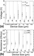
Resistive memory devices have the potential to replace flash technology due to their increased scalability, low voltage of operation, and compatibility with silicon semiconductor manufacturing. We report a spin-on resistive switching material, hydrogen silsesquioxane (HSQ), which is a commonly used electron beam resist. We demonstrate device scalability from 100 μm to 48 nm and show that the switching properties do not depend on the device size. Set voltages were typically <3 V, while reset voltages were <1 V when analyzing the positive unipolar switching properties of these devices. The ratio of the high resistance to the low resistance was ranged from 101 to 102, creating a distinct memory window between the memory states. Composition–depth profiling revealed that copper from the bottom electrode migrated into the HSQ films as a result of annealing. It is therefore speculated that copper may play a role in the switching properties of devices based on this material.

Type
Articles
Copyright
Copyright © Materials Research Society 2012

Access options

Get access to the full version of this content by using one of the access options below. (Log in options will check for institutional or personal access. Content may require purchase if you do not have access.)

References

REFERENCES

Waser, R., Dittmann, R., Staikov, G., and Szot, K.: Redox-based resistive switching memories - nanoionic mechanisms, prospects, and challenges. Adv. Mater. 21, 26322663 (2009).CrossRefGoogle ScholarPubMed
Pershin, Y.V. and Di Ventra, M.: Memory effects in complex materials and nanoscale systems. Adv. Phys. 60, 145227 (2011).CrossRefGoogle Scholar
Ouyang, J.: Application of nanomaterials in two-terminal resistive-switching memory devices. Nano Rev. 1, 114 (2010).CrossRefGoogle ScholarPubMed
Sawa, A.: Resistive switching in transition metal oxides. Mater. Today 11, 2836 (2008).CrossRefGoogle Scholar
Wang, R.Y., Tangirala, R., Raoux, S., Jordan-Sweet, J.L., and Milliron, D.J.: Ionic and electronic transport in Ag2S nanocrystal-GeS2 matrix composites with size-controlled Ag2S nanocrystals. Adv. Mater. 24, 99103 (2012).CrossRefGoogle ScholarPubMed
Kwon, D-H., Kim, K.M., Jang, J.H., Jeon, J.M., Lee, M.H., Kim, G.H., Li, X-S., Park, G-S., Lee, B., Han, S., Kim, M., and Hwang, C.S.: Atomic structure of conducting nanofilaments in TiO2 resistive switching memory. Nat. Nanotechnol. 5, 148153 (2010).CrossRefGoogle ScholarPubMed
Briggs, B.D., Bishop, S.M., Capulong, J.O., Hovish, M.Q., Matyi, R.J., and Cady, N.C.: Comparison of HfOx-based resistive memory devices with crystalline and amorphous active layers. Semiconductor Device Research Symposium (ISDRS), 2011 International. 7–9 Dec. 2011, pp. 1–2.CrossRefGoogle Scholar
Miao, F., Strachan, J.P., Yang, J.J., Zhang, M-X., Goldfarb, I., Torrezan, A.C., Eschbach, P., Kelley, R.D., Medeiros-Ribeiro, G., and Williams, R.S.: Anatomy of a nanoscale conduction channel reveals the mechanism of a high-performance memristor. Adv. Mater. 23, 56335640 (2011).CrossRefGoogle ScholarPubMed
Qi, J., Olmedo, M., Ren, J., Zhan, N., Zhao, J., Zheng, J-G., and Liu, J.: Resistive switching in single epitaxial ZnO nanoislands. ACS Nano. 6, 10511058 (2012).CrossRefGoogle ScholarPubMed
Van Nostrand, J.E., Cortez, R., Rice, Z.P., Cady, N.C., and Bergkvist, M.: Local transport properties, morphology and microstructure of ZnO decorated SiO2 nanoparticles. Nanotechnology 21, 415602 (2010).CrossRefGoogle ScholarPubMed
Linn, E., Rosezin, R., Kügeler, C., and Waser, R.: Complementary resistive switches for passive nanocrossbar memories. Nat. Mater. 9, 403406 (2010).CrossRefGoogle ScholarPubMed
Bishop, S.M., Bakhru, H., Novak, S.W., Briggs, B.D., Matyi, R.J., and Cady, N.C.: Ion implantation synthesized copper oxide-based resistive memory devices. Appl. Phys. Lett. 99, 202102 (2011).CrossRefGoogle Scholar
Cagli, C., Nardi, F., and Ielmini, D.: Modeling of set/reset operations in NiO-based resistive-switching memory devices. IEEE Trans. Electron Devices 56, 17121720 (2009).CrossRefGoogle Scholar
Schindler, C., Thermadam, S.C.P., Waser, R., and Kozicki, M.N.: Bipolar and unipolar resistive switching in Cu-doped SiO2. IEEE Trans. Electron Devices 54, 27622768 (2007).CrossRefGoogle Scholar
Simmons, J.G. and Verderber, R.R.: New conduction and reversible memory phenomena in thin insulating films. Proc. R. Soc. A: Math. Phys. Eng. Sci. 301, 77102 (1967).Google Scholar
Furuta, S., Takahashi, T., Naitoh, Y., Horikawa, M., Shimizu, T., and Ono, M.: Dependence of electric properties of a nanogap junction on electrode material. Jpn. J. Appl. Phys. 47, 18061812 (2008).CrossRefGoogle Scholar
Meier, M., Gilles, S., Rosezin, R., Schindler, C., Trellenkamp, S., Rüdiger, A., Mayer, D., Kügeler, C., and Waser, R.: Resistively switching Pt/spin-on glass/Ag nanocells for non-volatile memories fabricated with UV nanoimprint lithography. Microelectron. Eng. 86, 10601062 (2009).CrossRefGoogle Scholar
Rosezin, R., Meier, M., Breuer, U., Kügeler, C., and Waser, R.: Electroforming and resistance switching characteristics of silver-doped MSQ with inert electrodes. IEEE Trans. Nanotechnol. 10, 338343 (2011).CrossRefGoogle Scholar
Yao, J., Sun, Z., Zhong, L., Natelson, D., and Tour, J.M.: Resistive switches and memories from silicon oxide. Nano Lett. 10, 41054110 (2010).CrossRefGoogle ScholarPubMed
Yao, J., Zhong, L., Natelson, D., and Tour, J.M.: Intrinsic resistive switching and memory effects in silicon oxide. Appl. Phys. A. 102, 835839 (2011).CrossRefGoogle Scholar
Yao, J., Zhong, L., Natelson, D., and Tour, J.M.: Etching-dependent reproducible memory switching in vertical SiO2 structures. Appl. Phys. Lett. 93, 253101 (2008).CrossRefGoogle Scholar
Mehonic, A., Cueff, S., Wojdak, M., Hudziak, S., Jambois, O., Labbé, C., Garrido, B., Rizk, R., and Kenyon, A.J.: Resistive switching in silicon suboxide films. J. Appl. Phys. 111, 074507 (2012).CrossRefGoogle Scholar
Schindler, C., Weides, M., Kozicki, M.N., and Waser, R.: Low current resistive switching in Cu–SiO2 cells. Appl. Phys. Lett. 92, 122910 (2008).CrossRefGoogle Scholar
Kim, S., Jeong, H.Y., Kim, S.K., Choi, S-Y., and Lee, K.J.: Flexible memristive memory array on plastic substrates. Nano Lett. 11, 54385442 (2011).CrossRefGoogle ScholarPubMed
Yang, C-C. and Chen, W-C.: The structures and properties of hydrogen silsesquioxane (HSQ) films produced by thermal curing. J. Mater. Chem. 12, 11381141 (2002).CrossRefGoogle Scholar
Bornhauser, P. and Calzaferri, G.: Ring-opening vibrations of spherosiloxanes. J. Phys. Chem. 100, 20352044 (1996).CrossRefGoogle Scholar
Marcolli, C., Lainé, P., Bühler, R., Calzaferri, G., and Tomkinson, J.: Vibrations of H8Si8O12, D8Si8O12, and H10Si10O15 as determined by INS, IR, and Raman experiments. J. Phys. Chem. B. 101, 11711179 (1997).CrossRefGoogle Scholar
Kim, K.M., Jeong, D.S., and Hwang, C.S.: Nanofilamentary resistive switching in binary oxide system; a review on the present status and outlook. Nanotechnology 22, 254002 (2011).CrossRefGoogle ScholarPubMed
Kim, K.M., Choi, B.J., Koo, B.W., Choi, S., Jeong, D.S., and Hwang, C.S.: Resistive switching in Pt/Al2O3/TiO2/Ru stacked structures. Electrochem. Solid-State Lett. 9, G343G346 (2006).CrossRefGoogle Scholar
Loke, A.L.S., Yue, C.P., Cho, J.S.H., and Wong, S.S.: Kinetics of copper drift in PECVD dielectrics. IEEE Electron Device Lett. 17, 549551 (1996).CrossRefGoogle Scholar
Thermadam, S.P., Bhagat, S.K., Alford, T.L., Sakaguchi, Y., Kozicki, M.N., and Mitkova, M.: Influence of Cu diffusion conditions on the switching of Cu–SiO2-based resistive memory devices. Thin Solid Films 518, 32933298 (2010).CrossRefGoogle Scholar
Willis, B.G. and Lang, D.V.: Oxidation mechanism of ionic transport of copper in SiO2 dielectrics. Thin Solid Films 467, 284293 (2004).CrossRefGoogle Scholar
He, M. and Lu, T-M.: Metal-dielectric interfaces in gigascale electronics. In Chapter 2 Metal–Dielectric Diffusion Processes: Fundamentals, R. Hull, C. Jagadish, R.M. Osgood, J. Parisi, and Z.M. Wang, eds. Vol. 157 (Springer, New York, NY, 2012); pp. 1122.Google Scholar
Zhi-yong, P. and Ming-pu, W.: Thermomechanical treatment of super high strength Cu-8.0Ni-1.8Si alloy. Trans. Nonferrous Met. Soc. China 17, S1076S1080 (2007).Google Scholar
Stobrawa, J., Rdzawski, Z., Głuchowski, W., and Malec, W.: Ultrafine grained strips of precipitation hardened copper alloys. Arch. Metall. Mater. 56, 171179 (2011).CrossRefGoogle Scholar