Hostname: page-component-78c5997874-4rdpn Total loading time: 0 Render date: 2024-11-09T20:33:29.276Z Has data issue: false hasContentIssue false

Characteristics of direct-patternable SnO2:Pt nanocomposite thin films fabricated by photochemical metal-organic deposition

Published online by Cambridge University Press:  17 October 2011
Yong-June Choi
Affiliation:
Department of Materials Science and Engineering, Yonsei University, Seoul 120-749, Korea
Chae-Jung Kim
Affiliation:
Department of Materials Science and Engineering, Yonsei University, Seoul 120-749, Korea
Hyung-Ho Park*
Affiliation:
Department of Materials Science and Engineering, Yonsei University, Seoul 120-749, Korea
*
a)Address all correspondence to this author. e-mail: [email protected]
Get access

Abstract

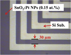
We evaluated the optical and electrical characteristics of SnO2 hybrid films with various contents (0, 0.05, 0.1, 0.15, and 0.2 at.%) of Pt nanoparticles. The Pt nanoparticles were synthesized by a methanol reduction method, and their size was restricted to an average of 3 nm using poly(N-vinyl-2-pyrrolidone) as a protecting agent. An enhancement in electrical properties was observed due to the addition of Pt nanoparticles; the lowest resistivity (1.36 × 10⁻² Ω·cm) and the highest figure of merit (1.18 × 10⁻⁴ Ω−1) were obtained with SnO2 film containing 0.15 at.% Pt nanoparticles after annealing at 600 °C, and the average transmittance in the visible region was 86.61%. Well-defined 30-μm-wide direct-patterned SnO2 films containing Pt nanoparticles were formed by photochemical metal-organic deposition through a simple process including a photosensitive starting precursor, ultraviolet exposure, and removal of the unexposed area with solvent rinsing.

Type
Articles
Copyright
Copyright © Materials Research Society 2011

Access options

Get access to the full version of this content by using one of the access options below. (Log in options will check for institutional or personal access. Content may require purchase if you do not have access.)

References

REFERENCES

1.Zhang, W., Zhu, R., Liu, X., Liu, B., and Ramakrishna, S.: Facile construction of nanofibrous ZnO photoelectrode for dye-sensitized solar cell applications. Appl. Phys. Lett. 95, 043304 (2009).CrossRefGoogle Scholar
2.Vaufrey, D., Ben Khalifa, M., Besland, M.P., Sandu, C., Blanchin, M.G., Teodorescu, V., Roger, J.A., and Tardy, J.: Reactive ion etching of sol-gel-processed SnO2 transparent conducting oxide as a new materials for organic light emitting diodes. Synth. Met. 127, 207 (2002).CrossRefGoogle Scholar
3.Wager, J.F., Keszler, D.A., and Presley, R.E.: Transparent Electronics (Springer, New York, 2008).Google Scholar
4.Kim, H., Horowitz, J.S., Kim, W.H., Makinen, A.J., Kafafi, Z.H., and Chrisey, D.B.: Doped ZnO thin films as anode materials for organic light-emitting diodes. Thin Solid Films. 420, 539 (2002).CrossRefGoogle Scholar
5.Minami, T., Nanto, H., and Takata, S.: Highly conductive and transparent aluminum doped zinc oxide thin films prepared by RF magnetron sputtering. Jpn. J. Appl. Phys. 23, L280 (1984).CrossRefGoogle Scholar
6.Fan, H. and Reid, S.A.: Phase transformations in pulsed laser deposited nanocrystalline tin oxide thin films. Chem. Mater. 15, 564 (2003).CrossRefGoogle Scholar
7.Tiburcio-Silver, A. and Sanchez-Juarez, A.: SnO2:Ga thin films as oxygen gas sensor. Mater. Sci. Eng., B. 110, 268 (2004).CrossRefGoogle Scholar
8.Zhi, X., Zhao, G., Zhu, T., and Li, Y.: The morphological, optical and electrical properties of SnO2:F thin films prepared by spray pyrolysis. Surf. Interface Anal. 40, 67 (2008).CrossRefGoogle Scholar
9.Volokitin, Y., Sinzig, J., De Jongh, L.J., Schmid, G., Vargaftik, M.N., and Moiseev, I.I.: Quantum-size effects in the thermodynamic properties of metallic nanoparticles. Nature 384, 621 (1996).CrossRefGoogle Scholar
10.Colvin, V.L., Schlamp, M.C., and Alivisatos, A.P.: Light-emitting diodes made from cadmium selenide nanocrystals and a semiconducting polymer. Nature 370, 354 (1994).CrossRefGoogle Scholar
11.Pileni, M.P.: Reverse micelles as microreactors. J. Phys. Chem. 97, 6961 (1993).CrossRefGoogle Scholar
12.Kreibig, U. and Vollmer, M.: Optical Properties of Metal Clusters (Springer, Berlin, 1995).CrossRefGoogle Scholar
13.Stepanov, A.L. and Hole, D.E.: Recent Research and Development in Applied Physics, edited by Pandalai, A. (Transword Research Network, Kuala, 2002), Vol. 5, p. 1.Google Scholar
14.Houlton, D.J., Jones, A.C., Haycock, P.W., Williams, E.W., Bull, J., and Critchlow, G.W.: The deposition of platinum-containing tin oxide thin films by metal-organic CVD. Chem. Vap. Deposition 1, 26 (1995).CrossRefGoogle Scholar
15.Amjoud, M. and Maury, F.: MOCVD and properties of in situ doped Pt-SnO2 thin films. J. Phys. IV 09, Pr8-643 (1999).Google Scholar
16.Kim, S.H., Lee, K.T., Moon, J.H., and Lee, B.-T.: Effects of Pt/Pd co-doping on the sensitivity of SnO2 thin film sensors. Jpn. J. Appl. Phys. 41, L1002 (2002).CrossRefGoogle Scholar
17.Ivanov, P., Llobet, E., Vilanova, X., Brezmes, J., Hubalek, J., and Correig, X.: Development of high sensitivity ethanol gas sensors based on Pt-doped SnO2 surfaces. Sens. Actuators, B 99, 201 (2004).CrossRefGoogle Scholar
18.D’Arienzo, M., Armelao, L., Cacciamani, A., Mari, C.M., Polizzi, S., Ruffo, R., Scotti, R., Testino, A., Wahba, L., and Morazzoni, F.: One-step preparation of SnO2 and Pt-doped SnO2 as inverse opal thin films for gas sensing. Chem. Mater. 22, 4083 (2010).CrossRefGoogle Scholar
19.Esfandyarpour, B., Mohajerzadeh, S., Famini, S., Khodadadi, A., and Soleimani, E.A.: High sensitivity Pt-doped SnO2 gas sensors fabricated using sol–gel solution on micromachined (100) Si substrates. Sens. Actuators, B 100, 190 (2004).CrossRefGoogle Scholar
20.Tadeev, A.V., Delabouglise, G., and Labeau, M.: Sensor properties of Pt doped SnO2 thin films for detecting CO. Thin Solid Films. 337, 163 (1999).CrossRefGoogle Scholar
21.Pierre, A.C.: Introduction to Sol-Gel Processing (Kluwer Academic Publishers, Norwell, MA, 2002), pp. 19.Google Scholar
22.Lee, J.K., Kim, T-Y., Chung, I., and Desu, S.B.: Characterization and elimination of dry etching damaged layer in Pt/Pb(Zr0.53Ti0.47)O3/Pt ferroelectric capacitor. Appl. Phys. Lett. 75, 334 (1999).CrossRefGoogle Scholar
23.Choi, Y-J., Park, H-H., Kim, H., Park, H-H., Chang, H.J., and Jeon, H.: Fabrication and characterization of direct-patternable ZnO films containing Pt nanoparticles. Jpn. J. Appl. Phys. 48, 035504 (2009).CrossRefGoogle Scholar
24.Park, H-H., Jung, S-B., Park, H-H., Kim, T.S., and Hill, R.H.: Electrical and ferroelectric properties of SBT thin films formed by photochemical metal-organic deposition. Sens. Actuators, B 126, 289 (2007).CrossRefGoogle Scholar
25.Teranishi, T., Hosoe, M., Tanaka, T., and Miyake, M.: Size control of monodispersed Pt nanoparticles and their 2D organization by electrophoretic deposition. J. Phys. Chem. B. 103, 3818 (1999).CrossRefGoogle Scholar
26.Choi, Y-J., Park, H-H., Golledge, S., Johnson, D.C., Chang, H.J., and Jeon, H.: The electrical and optical properties of direct-patternable SnO2 thin films containing Pt nanoparticles at various annealing temperatures. Surf. Coat. Technol. 205, 2649 (2010).CrossRefGoogle Scholar
27.Cullity, B.D. and Stock, S.R.: Elements of X-ray Diffraction, 3rd ed. (Prentice Hall, Upper Saddle River, NJ, 2001), pp. 170.Google Scholar
28.Du, Y.K., Yang, P., Mou, Z.G., Hua, N.P., and Jiang, L.: Thermal decomposition behaviors of PVP coated on platinum nanoparticles. J. Appl. Polym. Sci. 99, 23 (2006).CrossRefGoogle Scholar
29.Labeau, M., Gautheron, B., Cellier, F., Vallet-Regi, M., Garcia, E., and Calbet, J.M.G.: Pt nanoparticles dispersed on SnO2 thin films: A microstructural study. J. Solid State Chem. 102, 434 (1993).CrossRefGoogle Scholar
30.Qu, S., Song, Y., Liu, H., Wang, Y., Gao, Y., Liu, S., Zhang, X., Li, Y., and Zhu, D.: A theoretical and experimental study on optical limiting in platinum nanoparticles. Opt. Commun. 203, 283 (2002).CrossRefGoogle Scholar
31.Kryshtab, T.G., Palacios Gómez, J., and Mazin, M.O.: Phenomenon of primary and secondary extinction in textured materials. Rev. Mex. Fis. 48, 100 (2002).Google Scholar
32.Tan, S.T., Chen, B.J., Sun, X.W., Fan, W.J., Kwok, H.S., Zhang, X.H., and Chua, S.J.: Blueshift of optical band gap in ZnO thin films grown by metal-organic chemical-vapor deposition. J. Appl. Phys. 98, 013505 (2005).CrossRefGoogle Scholar
33.Spence, W.: The UV absorption edge of tin oxide thin films. J. Appl. Phys. 38, 3767 (1967).CrossRefGoogle Scholar
34.Burstein, E.: Anomalous optical absorption limit in InSb. Phys. Rev. 93, 632 (1954).CrossRefGoogle Scholar
35.Moss, T.S.: The interpretation of the properties of indium antimonide. Proc. Phys. Soc. London, Sect. B 67, 775 (1954).CrossRefGoogle Scholar
36.Ansari, S.G., Dar, M.A., Dhage, M.S., Kim, Y.S., Ansari, Z.A., Al-Hajry, A., and Shin, H-S.: A novel method for preparing stoichiometric SnO2 thin films at low temperature. Rev. Sci. Instrum. 80, 045112 (2009).CrossRefGoogle ScholarPubMed
37.Liu, P.Y., Chen, J.F., and Sun, W.D.: Characterizations of SnO2 and SnO2:Sb thin films prepared by PECVD. Vacuum 76, 7 (2004).CrossRefGoogle Scholar
38.Itoh, E., Iwamoto, M., Burghard, M., and Roth, S.: Ultraviolet photoelectron spectroscopy and surface potential of π-conjugated Langmuir-Blodgett films on gold metal electrode. Jpn. J. Appl. Phys. 39, 5146 (2000).CrossRefGoogle Scholar
39.Gupta, N. and Tyagi, B.P.: Effect of grain size on the mobility and transfer characteristics of polysilicon thin-film transistors. Indian. J. Pure Appl. Phys. 42, 528 (2004).Google Scholar
40.Haacke, G.: New figure of merit for transparent conductors. J. Appl. Phys. 47, 4086 (1976).CrossRefGoogle Scholar
41.Thangaraju, B.: Structural and electrical studies on highly conducting spray deposited fluorine and antimony doped SnO2 thin films from SnCl2 precursor. Thin Solid Films 402, 4357 (1971).Google Scholar