Hostname: page-component-586b7cd67f-2brh9 Total loading time: 0 Render date: 2024-11-26T04:48:04.624Z Has data issue: false hasContentIssue false

Thermally induced damages of PECVD SiNx thin films

Published online by Cambridge University Press:  25 August 2011

Yinong Liu*
Affiliation:
School of Mechanical and Chemical Engineering, The University of Western Australia, Crawley, Western Australia 6009, Australia
Neerushana Jehanathan
Affiliation:
School of Mechanical and Chemical Engineering, The University of Western Australia, Crawley, Western Australia 6009, Australia
John Dell
Affiliation:
School of Electrical, Electronic and Computer Engineering, The University of Western Australia, Crawley, Western Australia 6009, Australia
*
a)Address all correspondence to this author. e-mail: [email protected]
Get access

Abstract

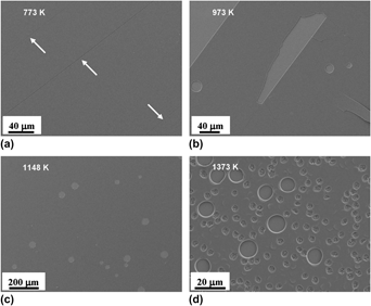
This study investigates thermally induced structural damages to amorphous plasma-enhanced chemical vapor deposition (PECVD) SiNx thin films at elevated temperatures, including chemical structure, microstructure, and physical integrity. The films were synthesized by means of PECVD method. Heating to elevated temperatures in air was found to cause multiple forms of chemical, structural, and physical damages. Chemically the films were found to oxidize and lose their nitrogen and hydrogen contents. Structurally the amorphous SiNx matrix was found to convert partially into SiO2 as a result of oxidation and to crystallize into Si3N4 crystallites. The physical damages include pinholes, circular “penny” cracks, random “dry mud” cracks, and spalling. The types of the damages were observed in different temperature regimes. The formation of the penny cracks is attributed to excessive compressive stresses created in the film by oxidation, which is associated with a large volume expansion. The formation of the random cracks is attributed to tensile stresses caused by crystallization, which is associated with a large volume contraction. Such damages limit the suitable application conditions for devices made of these films.

Type
Articles
Copyright
Copyright © Materials Research Society 2011

Access options

Get access to the full version of this content by using one of the access options below. (Log in options will check for institutional or personal access. Content may require purchase if you do not have access.)

References

REFERENCES

1.Ouacha, A., Willander, M., Hammarlund, B., and Logan, R.A.: Effect of surface passivation with SiN on the electrical properties of InP/InGaAs heterojunction bipolar transistors. J. Appl. Phys. 74, 5602 (1993).CrossRefGoogle Scholar
2.Brunet-Bruneau, A., Vuye, G., Frigerio, J.M., Abeles, F., Rivory, J., Berger, M., and Chaton, P.: Infrared ellipsometry investigation of SiOxNy thin films on silicon. Appl. Opt. 35, 4998 (1996).CrossRefGoogle ScholarPubMed
3.Santana, G., Fandino, J., Ortiz, A., and Alonso, J.C.: Low temperature–low hydrogen content silicon nitrides thin films deposited by PECVD using dichlorosilane and ammonia mixtures. J. Non-Cryst. Solids 351, 922 (2005).CrossRefGoogle Scholar
4.Antoszewski, J., Martyniuk, M., Musca, C.A., Dell, J.M., and Faraone, L.: Towards MEMS based infrared tunable micro-spectrometers. SPIE Proc. 1618, 148 (2002).CrossRefGoogle Scholar
5.Winchester, K.J. and Dell, J.M.: Tunable Fabry–P’erot cavities fabricated from PECVD silicon nitride employing zinc sulphide as the sacrificial layer. J. Micromech. Microeng. 11, 589 (2001).CrossRefGoogle Scholar
6.Soh, M.T.K., Savvides, N., Musca, C.A., Martyniuk, M.P., and Faraone, L.: Local bonding environment of nitrogen-rich silicon nitride thin films. J. Appl. Phys. 97, 093714 (2005).CrossRefGoogle Scholar
7.Bae, S., Farber, D.G., and Fonash, S.J.: Characteristics of low-temperature silicon nitride (SiNx:H) using electron cyclotron resonance plasma. Solid State Electron. 44, 1355 (2000).CrossRefGoogle Scholar
8.Karcher, R., Ley, L., and Johnson, R.L.: Electronic structure of hydrogenated and unhydrogenated amorphous SiNx: A photoemission study. Phys. Rev. B 30, 1896 (1984).CrossRefGoogle Scholar
9.Knolle, W.R. and Osenbach, J.W.: The structure of plasma deposited silicon nitride films determined by infrared spectroscopy. J. Appl. Phys. 58, 1248 (1985).CrossRefGoogle Scholar
10.Alvarez, F. and Valladares, A.A.: The atomic and electronic structure of amorphous silicon nitride. Rev. Mex. Fis. 48, 528 (2002).Google Scholar
11.Thurn, J., Cook, R.F., Kamarajugadda, M., Bozeman, S.P., and Stearns, L.C.: Stress hysteresis and mechanical properties of plasma-enhanced chemical vapor deposited dielectric films. J. Appl. Phys. 95, 967 (2004).CrossRefGoogle Scholar
12.Jehanathan, N., Liu, Y., Walmsley, B., Dell, J., and Saunders, M.: Effect of oxidation on the chemical bonding structure of PECVD SiNx thin films. J. Appl. Phys. 100, 123516 (2006).Google Scholar
13.Cordill, M.J., Bahr, D.F., Moody, N.R., and Gerberich, W.W.: Adhesion measurements using telephone cord buckles. Mater. Sci. Eng., A 443, 150 (2007).CrossRefGoogle Scholar
14.Coupeau, C., George, M., Regache, I., Colin, J., and Grilhe, J.: Buckling pattern with rings: Evidence of plastic damage in thin films. Philos. Mag. Lett. 83, 453 (2003).CrossRefGoogle Scholar
15.Hughey, M.P. and Cook, R.F.: Massive stress changes in plasma-enhanced chemical vapor deposited silicon nitride films on thermal cycling. Thin Solid Films 460, 7 (2004).Google Scholar
16.Jehanathan, N., Walmsley, B., Liu, Y., and Dell, J.: Oxidation of PECVD SiNx thin films. J. Alloy. Compd. 437, 332 (2007).CrossRefGoogle Scholar
17.Aydinli, A. and Ay, F.: Comparative investigation of hydrogen bonding in silicon based PECVD grown dielectrics for optical waveguides. Opt. Mater. 26, 33 (2004).Google Scholar
18.Kanata, T., Takakura, H., and Hamakawa, Y.: Preparation of composition-controlled silicon oxynitride films by sputtering; deposition mechanism, and optical and surface properties. Appl. Phys. A 49, 305 (1989).CrossRefGoogle Scholar
19.Ray, S.K., Das, S., Maiti, C.K., Lahiri, S.K., and Chakraborti, N.B.: Effect of reactive ion bombardment on the properties of silicon nitride and oxynitride films deposited by dual ion beam sputtering. J. Appl. Phys. 75, 8145 (1994).CrossRefGoogle Scholar
20.Jehanathan, N., Saunders, M., Liu, Y., and Dell, J.: Crystallization in silicon nitride thin films synthesised by plasma enhanced chemical vapour deposition. Scr. Mater. 57, 739 (2007).CrossRefGoogle Scholar
21.Audoly, B.: Stability of straight delamination blisters. Phys. Rev. Lett. 83, 4124 (1999).CrossRefGoogle Scholar
22.Walmsley, B.A., Liu, Y., Hu, X.Z., Bush, M.B., Winchester, K.J., Martyniuk, M., Dell, J.M., and Faraone, L.: Effects of deposition temperature on the mechanical and physical properties of PECVD silicon nitride thin films. J. Appl. Phys. 98, 044904 (2005).Google Scholar