Hostname: page-component-586b7cd67f-l7hp2 Total loading time: 0 Render date: 2024-11-26T07:06:43.491Z Has data issue: false hasContentIssue false

The Snomipede: A parallel platform for scanning near-field photolithography

Published online by Cambridge University Press:  25 November 2011

Ehtsham ul-Haq
Affiliation:
Department of Chemistry, University of Sheffield, Sheffield S3 7HF, United Kingdom
Zhuming Liu
Affiliation:
School of Pharmacy, University of Nottingham, Nottingham NG7 2RD, United Kingdom
Yuan Zhang
Affiliation:
Department of Electronics and Electrical Engineering, University of Glasgow, Glasgow G12 8LT, United Kingdom
Shahrul A. Alang Ahmad
Affiliation:
Department of Chemistry, Faculty of Science, Universiti Putra Malaysia, 43400 UPM Serdang, Selangor, Malaysia
Lu Shin Wong
Affiliation:
School of Chemistry and Manchester Interdisciplinary Biocentre, The University of Manchester, Manchester M1 7DN, United Kingdom
Jamie K. Hobbs
Affiliation:
Department of Physics and Astronomy, University of Sheffield, Sheffield S3 7RH, United Kingdom
Graham J. Leggett*
Affiliation:
Department of Chemistry, University of Sheffield, Sheffield S3 7HF, United Kingdom
Jason Micklefield
Affiliation:
School of Chemistry, The University of Manchester, Manchester M13 9PL, United Kingdom; and Manchester Interdisciplinary Biocentre, The University of Manchester, Manchester M1 7DN, United Kingdom
Clive J. Roberts
Affiliation:
School of Pharmacy, University of Nottingham, Nottingham NG7 2RD, United Kingdom
John M.R. Weaver
Affiliation:
Department of Electronics and Electrical Engineering, University of Glasgow, Glasgow G12 8LT, United Kingdom
*
a)Address all correspondence to this author. e-mail: [email protected]
Get access

Abstract

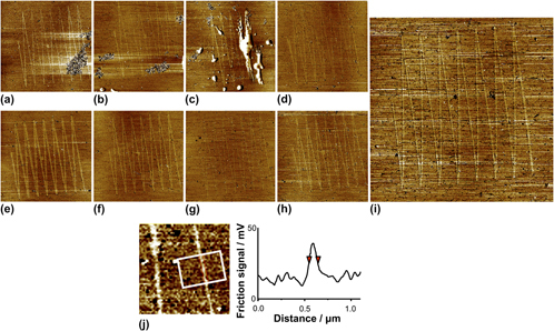
Using scanning near-field lithography (SNP), it is possible to pattern molecules at surfaces with a resolution as good as 9 nm [M. Montague, R. E. Ducker, K. S. L. Chong, R. J. Manning, F. J. M. Rutten, M. C. Davies and G. J. Leggett, Langmuir23 (13), 7328–7337 (2007)]. However, in common with other scanning probe techniques, SNP has previously been considered a serial process, hindering its use in many applications. IBM’s “Millipede” addresses this problem by utilizing an array of local probes operating in parallel. Here, we describe the construction of two instruments (Snomipedes) that integrate near-field optical methods into the parallel probe paradigm and promise the integration of top–down and bottom–up fabrication methods over macroscopic areas. Both are capable of performing near-field lithography with 16 probes in parallel spanning approximately 2 mm. The instruments can work in both ambient and liquid environments, key to many applications in nanobiology. In both, separate control of writing is possible for each probe. We demonstrate the deprotection of self-assembled monolayers of alkylsilanes with photocleavable protecting groups and subsequent growth of nanostructured polymer brushes from these nanopatterned surfaces by atom-transfer radical polymerization.

Type
Invited Feature Paper
Copyright
Copyright © Materials Research Society 2011

Access options

Get access to the full version of this content by using one of the access options below. (Log in options will check for institutional or personal access. Content may require purchase if you do not have access.)

References

REFERENCES

1.Steinmann, P. and Weaver, J.M.R.: Nanometer-scale gaps between metallic electrodes fabricated using a statistical alignment technique. Appl. Phys. Lett. 86, 063104 (2005).CrossRefGoogle Scholar
2.Zharnikov, M. and Grunze, M.: Modification of thiol-derived self-assembling monolayers by electron and x-ray irradiation: Scientific and lithographic aspects. J. Vac. Sci. Technol. B 20, 1793 (2002).CrossRefGoogle Scholar
3.Golzhauser, A., Eck, W., Geyer, W., Stadler, V., and Grunze, M.: Chemical nanolithography with electron beams. Adv. Mater. 13, 806 (2001).CrossRefGoogle Scholar
4.Ballav, N., Thomas, H., Winkler, T., Terfort, A., and Zharnikov, M.: Making Protein Patterns by Writing in a Protein-Repelling Matrix. Angew. Chem. Int. Ed. 48, 5833 (2009).CrossRefGoogle Scholar
5.Sun, S. and Leggett, G.J.: Matching the resolution of electron beam lithography by scanning near-field photolithography. Nano Lett. 4, 1381 (2004).CrossRefGoogle Scholar
6.Sun, S.Q., Chong, K.S.L., and Leggett, G.J.: Nanoscale molecular patterns fabricated by using scanning near-field optical lithography. J. Am. Chem. Soc. 124, 2414 (2002).CrossRefGoogle ScholarPubMed
7.Maoz, R., Frydman, E., Cohen, S.R., and Sagiv, J.: Constructive nanolithography: Site-defined silver self-assembly on nanoelectrochemically patterned monolayer templates. Adv. Mater. 12, 424 (2000).3.0.CO;2-S>CrossRefGoogle Scholar
8.Maoz, R., Frydman, E., Cohen, S.R., and Sagiv, J.: Constructive nanolithography: Inert monolayers as patternable templates for in-situ nanofabrication of metal-semiconductor-organic surface structures—A generic approach. Adv. Mater. 12, 725 (2000).3.0.CO;2-Z>CrossRefGoogle Scholar
9.Maoz, R., Cohen, S.R., and Sagiv, J.: Nanoelectrochemical patterning of monolayer surfaces: Toward spatially defined self-assembly of nanostructures. Adv. Mater. 11, 55 (1999).3.0.CO;2-8>CrossRefGoogle Scholar
10.Liu, M., Amro, N.A., Chow, C.S., and Liu, G-Y.: Production of nanostructures on DNA surfaces. Nano Lett. 2, 863 (2002).CrossRefGoogle Scholar
11.Liu, G-Y. and Amro, N.A.: Positioning protein molecules on surfaces: A nanoengineering approach to supramolecular chemistry. Proc. Natl. Acad. Sci. USA 99, 5165 (2002).CrossRefGoogle ScholarPubMed
12.Amro, N.A., Xu, S., and Liu, G-Y.: Patterning surfaces using tip-directed displacement and assembly. Langmuir 16, 3006 (2000).CrossRefGoogle Scholar
13.Lim, J-H., Ginger, D.S., Lee, K-B., Heo, J., Nam, J-M., and Mirkin, C.A.: Direct-write dip-pen nanolithography of proteins on modified silicon oxide surfaces. Angew. Chem. Int. Ed. 42, 2309 (2003).CrossRefGoogle ScholarPubMed
14.Lee, K-B., Park, S-J., Mirkin, C.A., Smith, J.C., and Mrksich, M.: Protein nanoarrays generated by dip-pen nanolithography. Science 295, 1702 (2002).CrossRefGoogle ScholarPubMed
15.Hong, S.H. and Mirkin, C.A.: A nanoplotter with both parallel and serial writing capabilities. Science 288, 1808 (2000).CrossRefGoogle ScholarPubMed
16.Hong, S.H., Zhu, J., and Mirkin, C.A.: Multiple ink nanolithography: Toward a multiple-pen nano-plotter. Science 286, 523 (1999).CrossRefGoogle Scholar
17.Piner, R.D., Zhu, J., Xu, F., Hong, S., and Mirkin, C.A.: Dip-pen nanolithography. Science 283, 661 (1999).CrossRefGoogle ScholarPubMed
18.Manoharan, H.C., Lutz, C.P., and Eigler, D.M.: Quantum mirages formed by coherent projection of electronic structure. Nature 403(6769), 512 (2000).CrossRefGoogle ScholarPubMed
19.Zhou, D., Bruckbauer, A., Ying, L.M., Abell, C., and Klenerman, D.: Building three-dimensional surface biological assemblies on the nanometer scale. Nano Lett. 3, 1517 (2003).CrossRefGoogle Scholar
20.Mateiu, R., Kuhle, A., Marie, R., and Boisen, A.: Building a multi-walled carbon nanotube-based mass sensor with the atomic force microscope. Ultramicrosc. 105, 233 (2005).CrossRefGoogle Scholar
21.Minne, S.C., Flueckiger, P., Soh, H.T., and Quate, C.F.: Atomic-force microscope lithography using amorphous-silicon as a resist and advances in parallel operation. J. Vac. Sci. Technol. B 13, 1380 (1995).CrossRefGoogle Scholar
22.Staii, C., Wood, D.W., and Scoles, G.: Ligand-induced structural changes in maltose binding proteins measured by atomic force microscopy. Nano Lett. 8, 2503 (2008).CrossRefGoogle ScholarPubMed
23.Gu, J.H., Yam, C.M., Li, S., and Cai, C.Z.: Nanometric protein arrays on protein-resistant monolayers on silicon surfaces. J. Am. Chem. Soc. 126, 8098 (2004).CrossRefGoogle ScholarPubMed
24.Fresco, Z.M. and Frechet, J.M.J.: Selective surface activation of a functional monolayer for the fabrication of nanometer scale thiol patterns and directed self-assembly of gold nanoparticles. J. Am. Chem. Soc. 127, 8302 (2005).CrossRefGoogle ScholarPubMed
25.Moyer, P.J., Walzer, K., and Hietschold, M.: Modification of the optical-properties of liquid-crystals using near-field Scanning optical microscopy. Appl. Phys. Lett. 67, 2129 (1995).CrossRefGoogle Scholar
26.Sun, S., Montague, M., Critchley, K., Chen, M-S., Dressick, W.J., Evans, S.D., and Leggett, G.J.: Fabrication of biological nanostructures by scanning near-field photolithography of chloromethylphenylsiloxane monolayers. Nano Lett. 6, 29 (2006).CrossRefGoogle ScholarPubMed
27.Reynolds, N.P., Tucker, J.D., Davison, P.A., Timney, J.A., Hunter, C.N., and Leggett, G.J.: Site-specific immobilization and micrometer and nanometer scale photopatterning of yellow fluorescent protein on glass surfaces. J. Am. Chem. Soc. 131, 896 (2009).CrossRefGoogle ScholarPubMed
28.Sun, S. and Leggett, G.J.: Micrometer and nanometer scale photopatterning of self-assembled monolayers of phosphonic acids on aluminum oxide. Nano Lett. 7, 3753 (2007).CrossRefGoogle Scholar
29.Sun, S., Mendes, P., Critchley, K., Diegoli, S., Hanwell, M., Evans, S.D., Leggett, G.J., Preece, J.A., and Richardson, T.H.: Fabrication of gold micro- and nanostructures by photolithographic exposure of thiol-stabilized gold nanoparticles. Nano Lett. 6, 345CrossRefGoogle Scholar
30.Montague, M., Ducker, R.E., Chong, K.S.L., Manning, R.J., Rutten, F.J.M., Davies, M.C., and Leggett, G.J.: Fabrication of biomolecular nanostructures by scanning near-field photolithography of oligo(ethylene glycol)-terminated self-assembled monolayers. Langmuir 23, 7328 (2007).CrossRefGoogle ScholarPubMed
31.Fodor, S.P., Read, J.L., Pirrung, M.C., Stryer, L., Lu, A.T., and Solas, D.: Light-directed, spatially addressable parallel chemical synthesis. Science 251, 767 (1991).CrossRefGoogle ScholarPubMed
32.Vettiger, P., Despont, M., Drechsler, U., Durig, U., Haberle, W., Lutwyche, M.I., Rothuizen, H.E., Stutz, R., Widmer, R., and Binnig, G.K.: The “Millipede”—More than one thousand tips for future AFM data storage. IBM J. Res. Develop. 44, 323 (2000).CrossRefGoogle Scholar
33.Minne, S.C., Yaralioglu, G., Manalis, S.R., Adams, J.D., Zesch, J., Atalar, A., and Quate, C.F.: Automated parallel high-speed atomic force microscopy. Appl. Phys. Lett. 72, 2340 (1998).CrossRefGoogle Scholar
34.Kingsley, J.W., Ray, S.K., Adawi, A.M., Leggett, G.J., and Lidzey, D.G.: Optical nanolithography using a scanning near-field probe with an integrated light source. Appl. Phys. Lett. 93, 213103 (2008).CrossRefGoogle Scholar
35.Zhang, Y., Docherty, K.E., and Weaver, J.M.R.: Batch fabrication of cantilever array aperture probes for scanning near-field optical microscopy. Microelectron. Eng. 87, 1229 (2010).CrossRefGoogle Scholar
36.Dufresne, E.R. and Grier, D.G.: Optical tweezer arrays and optical substrates created with diffractive optics. Rev. Sci. Instrum. 69, 1974 (1998).CrossRefGoogle Scholar
37.Curtis, J.E., Koss, B.A., and Grier, D.G.: Dynamic holographic optical tweezers. Opt. Commun. 207, 169 (2002).CrossRefGoogle Scholar
38.Ljungblad, U., Martinsson, H., and Sandstrom, T.: Phase shifted addressing using a spatial light modulator. Microelectron. Eng. 7879, 398 (2005).CrossRefGoogle Scholar
39.David, C., Kaulich, B., Medenwaldt, R., Hettwer, M., Fay, N., Diehl, M., Thieme, J., and Schmahl, G.: Low-distortion electron-beam lithography for fabrication of high-resolution germanium and tantalum zone plates. J. Vac. Sci. Technol. B 13, 2762 (1995).CrossRefGoogle Scholar
40.Djomehri, I.J., Savas, T.A., and Smith, H.I.: Zone-plate-array lithography in the deep ultraviolet. J. Vac. Sci. Technol. B 16, 3426 (1998).CrossRefGoogle Scholar
41.Ducker, R.E. and Leggett, G.J.: A mild etch for the fabrication of three-dimensional nanostructures in gold. J. Am. Chem. Soc. 128, 392 (2006).CrossRefGoogle ScholarPubMed
42.Brewer, N.J., Janusz, S.J., Critchley, K., Evans, S.D., and Leggett, G.J.: Photo-oxidation of self-assembled monolayers by exposure to light of wavelength 254 nm: A static SIMS study. J. Phys. Chem. B 109, 11247 (2005).CrossRefGoogle Scholar
43.Tizazu, G., Adawi, A., Leggett, G.J., and Lidzey, D.G.: Photopatterning, etching, and derivatization of self-assembled monolayers of phosphonic acids on the native oxide of titanium. Langmuir 25, 10746 (2009).CrossRefGoogle ScholarPubMed
44.Iqbal, P., Sun, S., Hanwell, M.D., Attwood, D., Leggett, G.J., Preece, J.A., Richardson, T.H., and Tunnicliffe, D.: Photochemical fabrication of three-dimensional micro- and nano-structured surfaces from a C60 monoadduct. J. Mater. Chem. 18, 2016 (2008).CrossRefGoogle Scholar
45.McGall, G., Labadie, J., Brock, P., Wallraff, G., Nguyen, T., and Hinsberg, W.: Light-directed synthesis of high-density oligonucleotide arrays using semiconductor photoresists. Proc. Natl. Acad. Sci. USA 93, 13555 (1996).CrossRefGoogle ScholarPubMed
46.McGall, G.H., Barone, A.D., Diggelmann, M., Fodor, S.P.A., Gentalen, E., and Ngo, N.: The efficiency of light-directed synthesis of DNA arrays on glass substrates. J. Am. Chem. Soc. 119, 5081 (1997).CrossRefGoogle Scholar
47.Sundberg, S.A., Barrett, R.W., Pirrung, M., Lu, A.L., Kiangsoontra, B., and Holmes, C.P.: Spatially-addressable immobilization of macromolecules on solid supports. J. Am. Chem. Soc. 117, 12050 (1995).CrossRefGoogle Scholar
48.Pirrung, M.C. and Huang, C-Y.: A general method for the spatially defined immobilization of biomolecules on glass surfaces using “caged” biotin. Bioconjugate Chem. 7, 317 (1996).CrossRefGoogle ScholarPubMed
49.Pirrung, M.C., Dore, T.M., Zhu, Y., and Rana, V.S.: Sensitized two-photon photochemical deprotection. Chem. Commun. 46, 5313 (2010).CrossRefGoogle ScholarPubMed
50.Pirrung, M.C., Wang, L., and Montague-Smith, M.P.: 3’-Nitrophenylpropyloxycarbonyl (NPPOC) protecting groups for high-fidelity automated 5’–3’ photochemical DNA synthesis. Org. Lett. 3, 1105 (2001).CrossRefGoogle Scholar
51.Alang Ahmad, S.A., Wong, L.S., Ul-Haq, E., Hobbs, J.K., Leggett, G.J., and Micklefield, J.: Micrometer- and nanometer-scale photopatterning using 2-nitrophenylpropyloxycarbonyl-protected aminosiloxane monolayers. J. Am. Chem. Soc. 131, 1513 (2009).CrossRefGoogle Scholar
52.Alang Ahmad, S.A., Wong, L.S., ul-Haq, E., Hobbs, J.K., Leggett, G.J. and Micklefield, J.: Protein micro- and nanopatterning using aminosilanes with protein-resistant photolabile protecting groups. J. Am. Chem. Soc. 133, 2749 (2011).CrossRefGoogle Scholar
53.Overney, R. and Meyer, E.: Tribological investigations using friction force microscopy. MRS Bull. 18, 26 (1993).CrossRefGoogle Scholar
54.Carpick, R.W. and Salmeron, M.: Scratching the surface: Fundamental investigations of tribology with atomic force microscopy. Chem. Rev. 97, 1163 (1997).CrossRefGoogle ScholarPubMed
55.Kaholek, M., Lee, W-K., Feng, J., LaMattina, B., Dyer, D.J., and Zauscher, S.: Weak polyelectrolyte brush arrays fabricated by combining electron-beam lithography with surface-initiated photopolymerization. Chem. Mater. 18, 3660 (2006).CrossRefGoogle Scholar
56.Riehn, R., Charas, A., Morgado, J., and Cacialli, F.: Near-field optical lithography of a conjugated polymer. Appl. Phys. Lett. 82, 526 (2003).CrossRefGoogle Scholar