Hostname: page-component-78c5997874-xbtfd Total loading time: 0 Render date: 2024-11-05T17:08:35.238Z Has data issue: false hasContentIssue false

Selective-area growth and transport properties of MnAs/InAs heterojunction nanowires

Published online by Cambridge University Press:  08 November 2019

Shinjiro Hara*
Affiliation:
Research Center for Integrated Quantum Electronics, Hokkaido University, Sapporo 060-0813, Japan
Matthias T. Elm
Affiliation:
Center for Materials Research, Justus Liebig University of Giessen, Giessen 35392, Germany; Institute of Experimental Physics I, Justus Liebig University of Giessen, Giessen 35392, Germany; and Institute of Physical Chemistry, Justus Liebig University of Giessen, Giessen 35392, Germany
Peter J. Klar
Affiliation:
Center for Materials Research, Justus Liebig University of Giessen, Giessen 35392, Germany; and Institute of Experimental Physics I, Justus Liebig University of Giessen, Giessen 35392, Germany
*
a)Address all correspondence to this author. e-mail: [email protected]
Get access

Abstract

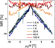
The authors summarize the results of selective-area growth of vertical MnAs/InAs heterojunction nanowire (NW) arrays and present a preliminary characterization of the transport properties of a single MnAs/InAs heterojunction NW and a single InAs host NW for MnAs inclusions. During the endotaxy of MnAs after the selective-area growth of host InAs nanowires (NWs) on partially SiO2-masked GaAs(111)B substrates, hexagonal NiAs-type MnAs nanoclusters (NCs), which exhibit spontaneous magnetization at room temperature, are formed with the 〈0001〉 direction oriented parallel to the 〈111〉B direction of the zinc-blende-type InAs host NWs. For InAs host NWs, a large positive ordinary magnetoresistance (MR) effect up to 165% is observed at temperatures between 7 and 280 K. In addition, magnetotransport measurements reveal universal conductance fluctuations and a weak Anderson localization at temperatures up to 20 K due to a charge-accumulation layer formed at the surface. Single MnAs/InAs heterojunction NWs, however, exhibit only a negative MR effect, which is independent of temperature T < 10 K and linearly decreases up to −10% at 10 T with increasing magnetic field. These results reveal the tremendous influence of ferromagnetic NCs on the transport behavior inside the InAs host NWs.

Type
Invited Paper
Copyright
Copyright © Materials Research Society 2019 

Access options

Get access to the full version of this content by using one of the access options below. (Log in options will check for institutional or personal access. Content may require purchase if you do not have access.)

References

Duan, X., Huang, Y., Cui, Y., Wang, J., and Lieber, C.M.: Indium phosphide nanowires as building blocks for nanoscale electronic and optoelectronic devices. Nature 409, 6669 (2001).CrossRefGoogle ScholarPubMed
Wang, J., Gudiksen, M.S., Duan, X., Cui, Y., and Lieber, C.M.: Highly polarized photoluminescence and photodetection from single indium phosphide nanowires. Science 293, 14551457 (2001).CrossRefGoogle ScholarPubMed
Cui, Y. and Lieber, C.M.: Functional nanoscale electronic devices assembled using silicon nanowire building blocks. Science 291, 851853 (2001).CrossRefGoogle ScholarPubMed
Thelander, C., Matensson, T., Björk, M.T., Ohlsson, B.J., Larsson, M.W., Wallenberg, L.R., and Samuelson, L.: Single-electron transistors in heterostructure nanowires. Appl. Phys. Lett. 83, 20522054 (2003).CrossRefGoogle Scholar
Duan, X., Huang, Y., Agarwal, R., and Lieber, C.M.: Single-nanowire electrically driven lasers. Nature 421, 241245 (2003).CrossRefGoogle ScholarPubMed
Zhang, D., Li, C., Liu, X., Han, S., Tang, T., and Zhou, C.: Doping dependent NH3 sensing of indium oxide nanowires. Appl. Phys. Lett. 83, 18451847 (2003).CrossRefGoogle Scholar
Offermans, P., Crego-Calama, M., and Brongersma, S.H.: Gas detection with vertical InAs nanowire arrays. Nano Lett. 10, 24122415 (2010).CrossRefGoogle ScholarPubMed
Tian, B., Zheng, X., Kempa, T.J., Fang, Y., Yu, N., Yu, G., Huang, J., and Lieber, C.M.: Coaxial silicon nanowires as solar cells and nanoelectronic power sources. Nature 449, 885890 (2007).CrossRefGoogle ScholarPubMed
Wallentin, J., Anttu, N., Asoli, D., Huffman, M., Åberg, I., Magnusson, M.H., Siefer, G., Fuss-Kailuweit, P., Dimroth, F., Witzigmann, B., Xu, H.Q., Samuelson, L., Deppert, K., and Borgström, M.T.: InP nanowire array solar cells achieving 13.8% efficiency by exceeding the ray optics limit. Science 339, 10571060 (2013).CrossRefGoogle ScholarPubMed
Han, N., Wang, F., Hou, J.J., Yip, S.P., Lin, H., Xiu, F., Fang, M., Yang, Z., Shi, X., Dong, G., Hung, T.F., and Ho, J.C.: Tunable electronic transport properties of metal-cluster-decorated III–V nanowire transistors. Adv. Mater. 25, 44454451 (2013).CrossRefGoogle ScholarPubMed
Hong, Y.J., Yang, J.W., Lee, W.H., Ruoff, R.S., Kim, K.S., and Fukui, T.: Van der Waals epitaxial double heterostructure: InAs/single-layer graphene/InAs. Adv. Mater. 25, 68476853 (2013).CrossRefGoogle Scholar
Ren, P., Hu, W., Zhang, Q., Zhu, X., Zhuang, X., Ma, L., Fan, X., Zhou, H., Liao, L., Duan, X., and Pan, A.: Band-selective infrared photodetectors with complete-composition-range InAsxP1−x alloy nanowires. Adv. Mater. 26, 74447449 (2014).CrossRefGoogle ScholarPubMed
Bao, T.H., Yakimets, D., Ryckaert, J., Ciofi, I., Baert, R., Veloso, A., Boemmels, J., Collaert, N., Roussel, P., Demuynck, S., Raghavan, P., Mercha, A., Tokei, Z., Verkest, D., Thean, A.V-Y., and Wambacq, P.: Circuit and process co-design with vertical gate-all-around nanowire FET technology to extend CMOS scaling for 5 nm and beyond technologies. In Proceedings of the 44th European Solid–State Device Research Conference ESSDERC 2014 , R. Bez, P. Pavan, and G. Meneghesso, eds. (IEEE, New York, 2014); pp. 102105.CrossRefGoogle Scholar
Sato, T., Kobayashi, Y., Motohisa, J., Hara, S., and Fukui, T.: SA-MOVPE of InGaAs nanowires and their compositions studied by micro-PL measurement. J. Cryst. Growth 310, 51115113 (2008).CrossRefGoogle Scholar
Tomioka, K., Motohisa, J., Hara, S., and Fukui, T.: Control of InAs nanowire growth directions on Si. Nano Lett. 8, 34753480 (2008).CrossRefGoogle Scholar
Tanaka, T., Tomioka, K., Hara, S., Motohisa, J., Sano, E., and Fukui, T.: Vertical surrounding gate transistors using single InAs nanowires grown on Si substrates. Appl. Phys. Express 3, 025003 (2010).CrossRefGoogle Scholar
Kobayashi, Y., Kohashi, Y., Hara, S., and Motohisa, J.: Selective-area growth of InAs nanowires with metal/dielectric composite mask and their application to vertical surrounding-gate field-effect transistors. Appl. Phys. Express 6, 045001 (2013).CrossRefGoogle Scholar
Dasgupta, N.P., Sun, J., Liu, C., Brittman, S., Andrews, S.C., Lim, J., Gao, H., Yan, R., and Yang, P.: Semiconductor nanowires-synthesis, characterization, and applications. Adv. Mater. 26, 21372184 (2014).CrossRefGoogle ScholarPubMed
Goktas, N.I., Wilson, P., Ghukasyan, A., Wagner, D., McNamee, S., and LaPierre, R.R.: Nanowires for energy: A review. Appl. Phys. Rev. 5, 041305 (2018).CrossRefGoogle Scholar
Li, Z., Tan, H.H., Jagadish, C., and Fu, L.: III–V semiconductor single nanowire solar cells: A review. Adv. Mater. Technol. 3, 1800005 (2018).CrossRefGoogle Scholar
Mokkapati, S. and Jagadish, C.: Review on photonic properties of nanowires for photovoltaics. Opt. Express 24, 1734517358 (2016).CrossRefGoogle ScholarPubMed
Eaton, S.W., Fu, A., Wong, A.B., Ning, C-Z., and Yang, P.: Semiconductor nanowire lasers. Nat. Rev. Mater. 1, 16028 (2016).CrossRefGoogle Scholar
Holzman, I. and Ivry, Y.: Superconducting nanowires for single-photon detection: Progress, challenges, and opportunities. Adv. Quantum Technol. 2, 1800058 (2019).CrossRefGoogle Scholar
Joyce, H.J., Boland, J.L., Davies, C.L., Baig, S.A., and Johnston, M.B.: A review of the electrical properties of semiconductor nanowires: Insights gained from terahertz conductivity spectroscopy. Semicond. Sci. Technol. 31, 103003 (2016).CrossRefGoogle Scholar
Wang, Z., Lee, S., Koo, K-I., and Kim, K.: Nanowire-based sensors for biological and medical applications. IEEE Trans. NanoBioscience 15, 186199 (2016).CrossRefGoogle ScholarPubMed
Doucey, M-A. and Carrara, S.: Nanowire sensors in cancer. Trends Biotechnol. 37, 8699 (2019).CrossRefGoogle Scholar
Li, Q., Lu, N., Wang, L., and Fan, C.: Advances in nanowire transistor-based biosensors. Small Methods 2, 1700263 (2018).CrossRefGoogle Scholar
Mikolajick, T., Heinzig, A., Trommer, J., Baldauf, T., and Weber, W.M.: The RFET—A reconfigurable nanowire transistor and its application to novel electronic circuits and systems. Semicond. Sci. Technol. 32, 043001 (2017).CrossRefGoogle Scholar
Lind, E.: High frequency III–V nanowire MOSFETs. Semicond. Sci. Technol. 31, 093005 (2016).CrossRefGoogle Scholar
Tang, J. and Wang, K.L.: Electrical spin injection and transport in semiconductor nanowires: Challenges, progress and perspectives. Nanoscale 7, 43254337 (2015).CrossRefGoogle Scholar
Gould, C., Pappert, K., Schmidt, G., and Molenkamp, L.W.: Magnetic anisotropies and (Ga, Mn)As-based spintronic devices. Adv. Mater. 19, 323340 (2007).CrossRefGoogle Scholar
Elm, M.T., Klar, P.J., Ito, S., and Hara, S.: Influence of ordered arrangements of cluster chains on the hopping transport in GaAs:Mn/MnAs hybrids at low temperatures. Phys. Rev. B 83, 235305 (2011).CrossRefGoogle Scholar
Michel, C., Elm, M.T., Goldlücke, B., Baranovskii, S.D., Thomas, P., Heimbrodt, W., and Klar, P.J.: Tailoring the magnetoresistance of MnAs/GaAs:Mn granular hybrid nanostructures. Appl. Phys. Lett. 92, 223119 (2008).CrossRefGoogle Scholar
Wellmann, P.J., Garcia, J.M., Fend, J-L., and Petroff, P.M.: Giant magnetoresistance in a low-temperature GaAs/MnAs nanoscale ferromagnet hybrid structure. Appl. Phys. Lett. 73, 32913293 (1998).CrossRefGoogle Scholar
Elm, M.T., Michel, C., Stehr, J., Hofmann, D.M., Klar, P.J., Ito, S., Hara, S., and Krug von Nidda, H-A.: Comparison of the magnetic properties of GaInAs/MnAs and GaAs/MnAs hybrids with random and ordered arrangements of MnAs nanoclusters. J. Appl. Phys. 107, 013701 (2010).CrossRefGoogle Scholar
Hai, P.N., Ohya, S., Tanaka, M., Barnes, S.E., and Maekawa, S.: Electromotive force and huge magnetoresistance in magnetic tunnel junctions. Nature 458, 489493 (2009).CrossRefGoogle Scholar
Hai, P.N., Ohya, S., and Tanaka, M.: Long spin-relaxation time in a single metal nanoparticle. Nat. Nanotechnol. 5, 593596 (2010).CrossRefGoogle Scholar
Tanaka, M., Ohya, S., and Hai, P.N.: Recent progress in III–V based ferromagnetic semiconductors: Band structure, Fermi level, and tunneling transport. Appl. Phys. Rev. 1, 011102 (2014).CrossRefGoogle Scholar
Radovanovic, P.V., Barrelet, C.J., Gradečak, S., Qian, F., and Lieber, C.M.: General synthesis of manganese-doped II–VI and III–V semiconductor nanowires. Nano Lett. 5, 14071411 (2005).CrossRefGoogle ScholarPubMed
Kim, H.S., Cho, Y.J., Kong, K.J., Kim, C.H., Chung, G.B., Park, J., Kim, J.Y., Yoon, J., Jung, M.H., Jo, Y., Kim, B., and Ahn, J.P.: Room-temperature ferromagnetic Ga1−xMnxAs (x ≤ 0.05) nanowires: Dependence of electronic structures and magnetic properties on Mn content. Chem. Mater. 21, 11371143 (2009).CrossRefGoogle Scholar
Borschel, C., Messing, M.E., Borgström, M.T., Paschoal, W. Jr., Wallentin, J., Kumar, S., Mergenthaler, K., Deppert, K., Canali, C.M., Pettersson, H., Samuelson, L., and Ronning, C.: A new route toward semiconductor nanospintronics: Highly Mn-doped GaAs nanowires realized by ion-implantation under dynamic annealing conditions. Nano Lett. 11, 39353940 (2011).CrossRefGoogle ScholarPubMed
Rudolph, A., Soda, M., Kiessling, M., Wojtowicz, T., Schuh, D., Wegscheider, W., Zweck, J., Back, C., and Reiger, E.: Ferromagnetic GaAs/GaMnAs core–shell nanowires grown by molecular beam epitaxy. Nano Lett. 9, 38603866 (2009).CrossRefGoogle ScholarPubMed
Yu, X., Wang, H., Pan, D., Zhao, J., Misuraca, J., von Molnár, S., and Xiong, P.: All zinc-blende GaAs/(Ga, Mn)As core–shell nanowires with ferromagnetic ordering. Nano Lett. 13, 15721577 (2013).CrossRefGoogle ScholarPubMed
Ramlan, D.G., May, S.J., Zheng, J.G., Allen, J.E., Wessels, B.W., and Lauhon, L.J.: Ferromagnetic self-assembled quantum dots on semiconductor nanowires. Nano Lett. 6, 5054 (2006).CrossRefGoogle ScholarPubMed
Wolff, M.F.H., Görlitz, D., Nielsch, K., Messing, M.E., and Deppert, K.: Synthesis and magnetic characterization of MnAs nanoparticles via nanoparticle conversion. Nanotechnology 22, 055602 (2011).CrossRefGoogle ScholarPubMed
Hilse, M., Takagaki, Y., Herfort, J., Ramsteiner, M., Herrmann, C., Breuer, S., Geelhaar, L., and Riechert, H.: Ferromagnet-semiconductor nanowire coaxial heterostructures grown by molecular-beam epitaxy. Appl. Phys. Lett. 95, 133126 (2009).CrossRefGoogle Scholar
Liang, J., Wang, J., Paul, A., Cooley, B.J., Rench, D.W., Dellas, N.S., Mohney, S.E., Engel-Herbert, R., and Samarth, N.: Measurement and simulation of anisotropic magnetoresistance in single GaAs/MnAs core/shell nanowires. Appl. Phys. Lett. 100, 182402 (2012).CrossRefGoogle Scholar
Choi, H-J., Seong, H-K., Chang, J., Lee, K-I., Park, Y-J., Kim, J-J., Lee, S-K., He, R., Kuykendall, T., and Yang, P.: Single-crystalline diluted magnetic semiconductor GaN:Mn nanowires. Adv. Mater. 17, 13511356 (2005).CrossRefGoogle Scholar
Seong, H-K., Kim, J-Y., Kim, J-J., Lee, S-C., Kim, S-R., Kim, U., Park, T-E., and Choi, H-J.: Room-temperature ferromagnetism in Cu doped GaN nanowires. Nano Lett. 7, 33663371 (2007).CrossRefGoogle ScholarPubMed
Lensch-Falk, J.L., Hemesath, E.R., and Lauhon, L.J.: Syntaxial growth of Ge/Mn-germanide nanowire heterostructures. Nano Lett. 8, 26692673 (2008).CrossRefGoogle ScholarPubMed
Tang, J., Wang, C-Y., Hung, M-H., Jiang, X., Chang, L-T., He, L., Liu, P-H., Yang, H-J., Tuan, H-Y., Chen, L-J., and Wang, K-L.: Ferromagnetic germanide in Ge nanowire transistors for spintronics application. ACS Nano 6, 57105717 (2012).CrossRefGoogle ScholarPubMed
Lin, Y-C., Chen, Y., Shailos, A., and Huang, Y.: Detection of spin polarized carrier in silicon nanowire with single crystal MnSi as magnetic contacts. Nano Lett. 10, 22812287 (2010).CrossRefGoogle ScholarPubMed
Li, X., Meng, G., Qin, S., Xu, Q., Chu, Z., Zhu, X., Kong, M., and Li, A-P.: Nanochannel-directed growth of multi-segment nanowire heterojunctions of metallic Au1−xGex and semiconducting Ge. ACS Nano 6, 831836 (2012).CrossRefGoogle ScholarPubMed
Hara, S., Kawamura, D., Iguchi, H., Motohisa, J., and Fukui, T.: Self-assembly and selective-area formation of ferromagnetic MnAs nanoclusters on lattice-mismatched semiconductor surfaces by MOVPE. J. Cryst. Growth 310, 23902394 (2008).CrossRefGoogle Scholar
Yatago, M., Iguchi, H., Sakita, S., and Hara, S.: Growth and characterization of MnAs nanoclusters embedded in GaAs nanowires by metal-organic vapor phase epitaxy. Jpn. J. Appl. Phys. 51, 02BH01 (2012).CrossRefGoogle Scholar
Hara, S., Sakita, S., and Yatago, M.: Selective-area growth and electrical characterization of hybrid structures between semiconducting GaAs nanowires and ferromagnetic MnAs nanoclusters. Jpn. J. Appl. Phys. 51, 11PE01 (2012).CrossRefGoogle Scholar
Elm, M.T., Klar, P.J., Ito, S., Hara, S., and Krug von Nidda, H-A.: Effect of the cluster magnetization on the magnetotransport at low temperatures in ordered arrays of MnAs nanoclusters on (111)B GaAs. Phys. Rev. B 84, 035309 (2011).CrossRefGoogle Scholar
Fischer, M., Elm, M.T., Sakita, S., Hara, S., and Klar, P.J.: Magnetoresistance effects and spin-valve-like behavior in an arrangement of two MnAs nanoclusters. Appl. Phys. Lett. 106, 032401 (2015).CrossRefGoogle Scholar
Zwanenburg, F.A., van der Mast, D.W., Heersche, H.B., Kouwenhoven, L.P., and Bakkers, E.P.A.M.: Electric field control of magnetoresistance in InP nanowires with ferromagnetic contacts. Nano Lett. 9, 27042709 (2009).CrossRefGoogle ScholarPubMed
Inokuchi, T., Marukame, T., Ishikawa, M., Sugiyama, H., and Saito, Y.: Electrical spin injection into n-GaAs channels and detection through MgO/CoFeB electrodes. Appl. Phys. Express 2, 023006 (2009).CrossRefGoogle Scholar
Jiang, X., Wang, R., Shelby, R.M., Macfarlane, R.M., Bank, S.R., Harris, J.S., and Parkin, S.S.P.: Highly spin-polarized room-temperature tunnel injector for semiconductor spintronics using MgO(100). Phys. Rev. Lett. 94, 056601 (2005).CrossRefGoogle Scholar
Sugahara, S. and Nitta, J.: Spin-transistor electronics: An overview and outlook. Proc. IEEE 98, 21242154 (2010).CrossRefGoogle Scholar
Biermann, K., Hernandez-Minguez, A., Hey, R., and Santos, P.V.: Electrically tunable electron spin lifetimes in GaAs(111)B quantum wells. J. Appl. Phys. 112, 083913 (2012).CrossRefGoogle Scholar
Kodaira, R., Hara, S., Kabamoto, K., and Fujimagari, H.: Synthesis and structural characterization of vertical ferromagnetic MnAs/semiconducting InAs heterojunction nanowires. Jpn. J. Appl. Phys. 55, 075503 (2016).CrossRefGoogle Scholar
Kabamoto, K., Kodaira, R., and Hara, S.: Magnetization in vertical MnAs/InAs heterojunction nanowires. J. Cryst. Growth 464, 8085 (2017).CrossRefGoogle Scholar
Kodaira, R., Kabamoto, K., and Hara, S.: Shape control of ferromagnetic MnAs nanoclusters exhibiting magnetization switching in vertical MnAs/InAs heterojunction nanowires. Jpn. J. Appl. Phys. 56, 06GH03 (2017).CrossRefGoogle Scholar
Kodaira, R., Horiguchi, R., and Hara, S.: Magnetization characterization of MnAs nanoclusters at close range in bended MnAs/InAs heterojunction nanowires. J. Cryst. Growth 507, 241245 (2019).CrossRefGoogle Scholar
Elm, M.T. and Hara, S.: Transport properties of hybrids with ferromagnetic MnAs nanoclusters and their potential for new magnetoelectronic devices. Adv. Mater. 26, 80798095 (2014).CrossRefGoogle ScholarPubMed
Bonev, I.: On the terminology of the phenomena of mutual crystal orientation. Acta Crystallogr., Sect. A 28, 508512 (1972).CrossRefGoogle Scholar
Hara, S., Fujimagari, H., Sakita, S., and Yatago, M.: Difference in formation of ferromagnetic MnAs nanoclusters on III–V semiconducting nanowire templates. Proc. SPIE 8820, 88200V (2013).Google Scholar
Braun, W., Trampert, A., Kaganaer, V.M., Jenichen, B., Satapathy, D.K., and Ploog, K.H.: Endotaxy of MnSb into GaSb. J. Cryst. Growth 301–302, 5053 (2007).CrossRefGoogle Scholar
Nateghi, N., Ménard, D., and Masut, R.A.: Large interface diffusion in endotaxial growth of MnP films on GaP substrates. J. Appl. Phys. 116, 133512 (2014).CrossRefGoogle Scholar
Hara, S. and Fukui, T.: Hexagonal ferromagnetic MnAs nanocluster formation on GaInAs/InP(111)B layers by metal-organic vapor phase epitaxy. Appl. Phys. Lett. 89, 113111 (2006).CrossRefGoogle Scholar
Hara, S., Lampalzer, M., Torunski, T., Volz, K., Treutmann, W., and Stolz, W.: Cluster formation and magnetic properties of Mn-incorporated (GaIn)As/InP layers grown by metal-organic vapor phase epitaxy. J. Cryst. Growth 261, 330335 (2004).CrossRefGoogle Scholar
Hubmann, J., Bauer, B., Körner, H.S., Furthmeier, S., Buchner, M., Bayreuther, G., Dirnberger, F., Schuh, D., Back, C.H., Zweck, J., Reiger, E., and Bougeard, D.: Epitaxial growth of room-temperature ferromagnetic MnAs segments on GaAs nanowires via sequential crystallization. Nano Lett. 16, 900905 (2016).CrossRefGoogle ScholarPubMed
Wirths, S., Weis, K., Winden, A., Sladek, K., Volk, C., Alagha, S., Weirich, T.E., von der Ahe, M., Hardtdegen, H., Lüth, H., Demarina, N., Grützmacher, D., and Schäpers, T.: Effect of Si-doping on InAs nanowire transport and morphology. J. Appl. Phys. 110, 053709 (2011).CrossRefGoogle Scholar
Voronina, T.I., Lagunova, T.S., Moiseev, K.D., Rozov, A.E., Sipovskaya, M.A., Stepanov, M.V., Sherstnev, V.V., and Yakovlev, Y.P.: Electrical properties of epitaxial indium arsenide and narrow band solid solutions based on it. Semiconductors 33, 719725 (1999).CrossRefGoogle Scholar
Blömers, C., Lepsa, M.I., Luysberg, M., Grützmacher, D., Lüth, H., and Schäpers, T.: Electronic phase coherence in InAs nanowires. Nano Lett. 11, 35503556 (2011).CrossRefGoogle ScholarPubMed
Estévez Hernández, S., Akabori, M., Sladek, K., Volk, C., Alagha, S., Hardtdegen, H., Pala, M.G., Demarina, N., Grützmacher, D., and Schäpers, T.: Spin-orbit coupling and phase coherence in InAs nanowires. Phys. Rev. B 82, 235303 (2010).CrossRefGoogle Scholar
Olsson, L.Ö., Andersson, C.B.M., Håkansson, M.C., Kanski, J., Ilver, L., and Karlsson, U.O.: Charge accumulation at InAs surfaces. Phys. Rev. Lett. 76, 36263629 (1996).CrossRefGoogle ScholarPubMed
Noguchi, M., Hirakawa, K., and Ikoma, T.: Intrinsic electron accumulation layers on reconstructed clean InAs(100) surfaces. Phys. Rev. Lett. 66, 22432246 (1991).CrossRefGoogle ScholarPubMed
Sun, J., Soh, Y-A., and Kosel, J.: Geometric factors in the magnetoresistance of n-doped InAs epilayers. J. Appl. Phys. 114, 203908 (2013).CrossRefGoogle Scholar
Wieder, H.H.: Transport coefficients of InAs epilayers. Appl. Phys. Lett. 25, 206208 (1974).CrossRefGoogle Scholar
McCarthy, J.P.: Preparation and properties of epitaxial InAs. Solid-State Electron 10, 649655 (1967).CrossRefGoogle Scholar
Tsuji, Y. and Okamoto, T.: Magnetotransport measurements on a damaged surface of p-type InAs and the annealing effect. Phys. Rev. B 70, 245316 (2004).CrossRefGoogle Scholar
Nedoluha, A. and Koch, K.M.: Zum mechanismus der widerstandsänderung im magnetfeld. Z. Phys. 132, 608620 (1952).CrossRefGoogle Scholar
Bergmann, G.: Weak localization in thin films: A time-of-flight experiment with conduction electrons. Phys. Rep. 107, 158 (1984).CrossRefGoogle Scholar
Lee, P.A., Stone, A.D., and Fukuyama, H.: Universal conductance fluctuations in metals: Effects of finite temperature, interactions, and magnetic field. Phys. Rev. B 35, 10391070 (1987).CrossRefGoogle ScholarPubMed
Washburn, S. and Webb, R.A.: Quantum transport in small disordered samples from the diffusive to the ballistic regime. Rep. Prog. Phys. 55, 13111383 (1992).CrossRefGoogle Scholar
Elm, M.T., Uredat, P., Binder, J., Ostheim, L., Schäfer, M., Hille, P., Müßener, J., Schörmann, J., Eickhoff, M., and Klar, P.J.: Doping-induced universal conductance fluctuations in GaN nanowires. Nano Lett. 15, 78227828 (2015).CrossRefGoogle ScholarPubMed
Yang, P-Y., Wang, L.Y., Hsu, Y-W., and Lin, J-J.: Universal conductance fluctuations in indium tin oxide nanowires. Phys. Rev. B 85, 085423 (2012).CrossRefGoogle Scholar
Uredat, P., Hille, P., Schoermann, J., Klar, P.J., Eickhoff, M., and Elm, M.T.: Consistent description of mesoscopic transport: Case study of current-dependent magnetoconductance in single GaN:Ge nanowires. Phys. Rev. B 100, 085409 (2019).CrossRefGoogle Scholar
Lin, J.J. and Bird, J.P.: Recent experimental studies of electron dephasing in metal and semiconductor mesoscopic structures. J. Phys.: Condens. Matter 14, R501R596 (2002).Google Scholar
Beenakker, C.W.J. and van Houten, H.: Quantum transport in semiconductor nanostructures. In Solid State Physics, Vol. 44: Semiconductor Heterostructures and Nanostructures, Ehrenreich, H. and Turnbull, D., eds. (Academic Press, London, U.K., 1991); pp. 1228.Google Scholar
Hansen, A.E., Björk, M.T., Fasth, C., Thelander, C., and Samuelson, L.: Spin relaxation in InAs nanowires studied by tunable weak antilocalization. Phys. Rev. B 71, 205328 (2005).CrossRefGoogle Scholar
Roulleau, P., Choi, T., Riedi, S., Heinzel, T., Shorubalko, I., Ihn, T., and Ensslin, K.: Suppression of weak antilocalization in InAs nanowires. Phys. Rev. B 81, 155449 (2010).CrossRefGoogle Scholar
Dhara, S., Solanki, H.S., Singh, V., Narayanan, A., Chaudhari, P., Gokhale, M., Bhattacharya, A., and Deshmukh, M.M.: Magnetotransport properties of individual InAs nanowires. Phys. Rev. B 79, 121311 (2009).CrossRefGoogle Scholar
Wang, L.B., Guo, J.K., Kang, N., Pan, D., Li, S., Fan, D., Zhao, J., and Xu, H.Q.: Phase-coherent transport and spin relaxation in InAs nanowires grown by molecule beam epitaxy. Appl. Phys. Lett. 106, 173105 (2015).CrossRefGoogle Scholar
Altshuler, B.L., Aronov, A.G., and Khmelnitsky, D.E.: Effects of electron–electron collisions with small energy transfers on quantum localisation. J. Phys. C: Solid State Phys. 15, 73677386 (1982).CrossRefGoogle Scholar
Alagha, S., Estévez Hernández, S., Blömers, C., Stoica, T., Calarco, R., and Schäpers, T.: Universal conductance fluctuations and localization effects in InN nanowires connected in parallel. J. Appl. Phys. 108, 113704 (2010).CrossRefGoogle Scholar
Blömers, C., Schäpers, T., Richter, T., Calarco, R., Lüth, H., and Marso, M.: Temperature dependence of the phase-coherence length in InN nanowires. Appl. Phys. Lett. 92, 132101 (2008).CrossRefGoogle Scholar
Liang, D., Sakr, M.R., and Gao, X.P.A.: One-dimensional weak localization of electrons in a single InAs nanowire. Nano Lett. 9, 17091712 (2009).CrossRefGoogle Scholar
Liang, D. and Gao, X.P.A.: Strong tuning of Rashba spin-orbit interaction in single InAs nanowires. Nano Lett. 12, 32633267 (2012).CrossRefGoogle ScholarPubMed
Okabayashi, J., Mizokawa, T., Sarma, D.D., Fujimori, A., Slupinski, T., Oiwa, A., and Munekata, H.: Electronic structure of In1−xMnxAs studied by photoemission spectroscopy: Comparison with Ga1−xMnxAs. Phys. Rev. B 65, 161203 (2002).CrossRefGoogle Scholar
Shen, G., Zhao, Y., Bai, Y., Yu, D., Liu, J., Xie, H., Dong, Z., Yang, J., Yang, F., and Wang, F.: Impurity band conduction in Mn-doped p type InAs single crystal. Mater. Sci. Semicond. Process. 84, 115118 (2018).CrossRefGoogle Scholar
Chiu, P.T., Blattner, A.J., May, S.J., and Wessels, B.W.: Optical properties of Mn-doped InAs and InMnAs epitaxial films. Phys. J. B 344, 379384 (2004).CrossRefGoogle Scholar
Iye, Y., Oiwa, A., Endo, A., Katsumoto, S., Matsukura, F., Shen, A., Ohno, H., and Munekata, H.: Metal-insulator transition and magnetotransport in III–V compound diluted magnetic semiconductors. Mater. Sci. Eng., B 63, 8895 (1999).CrossRefGoogle Scholar
Ohno, H., Munekata, H., Penney, T., von Molnár, S., and Chang, L.L.: Magnetotransport properties of p-type (In,Mn)As diluted magnetic III–V semiconductors. Phys. Rev. Lett. 68, 26642667 (1992).CrossRefGoogle ScholarPubMed
Michel, C., Baranovskii, S.D., Thomas, P., Heimbrodt, W., Elm, M.T., Klar, P.J., Goldlücke, B., Wurstbauer, U., Reinwald, M., and Wegscheider, W.: Quantitative modeling of the annealing-induced changes of the magnetotransport in Ga1−xMnxAs alloys. J. Appl. Phys. 102, 073712 (2007).CrossRefGoogle Scholar
Ohno, H.: Making nonmagnetic semiconductors ferromagnetic. Science 281, 951956 (1998).CrossRefGoogle ScholarPubMed
Edmonds, K.W., Campion, R.P., Wang, K-Y., Neumann, A.C., Gallagher, B.L., Foxon, C.T., and Main, P.C.: Magnetoresistance and Hall effect in the ferromagnetic semiconductor Ga1−xMnxAs. J. Appl. Phys. 93, 67876789 (2003).CrossRefGoogle Scholar
May, S.J., Blattner, A.J., and Wessels, B.W.: Negative magnetoresistance in (In,Mn)As semiconductors. Phys. Rev. B 70, 073303 (2004).CrossRefGoogle Scholar
Michel, C., Klar, P.J., Baranovskii, S.D., and Thomas, P.: Influence of magnetic-field-induced tuning of disorder and band structure on the magnetoresistance of paramagnetic dilute magnetic semiconductors. Phys. Rev. B 69, 165211 (2004).CrossRefGoogle Scholar
Paschoal, W., Kumar, S., Borschel, C., Wu, P., Canali, C.M., Ronning, C., Samuelson, L., and Pettersson, H.: Hopping conduction in Mn ion-implanted GaAs nanowires. Nano Lett. 12, 48384842 (2012).CrossRefGoogle ScholarPubMed
Kumar, S., Paschoal, W. Jr., Johannes, A., Jacobsson, D., Borschel, C., Pertsova, A., Wang, C-H., Wu, M-K., Canali, C.M., Ronning, C., Samuelson, L., and Pettersson, H.: Magnetic polarons and large negative magnetoresistance in GaAs nanowires implanted with Mn ions. Nano Lett. 13, 50795084 (2013).CrossRefGoogle ScholarPubMed
Matsukura, F., Ohno, H., Shen, A., and Sugawara, Y.: Transport properties and origin of ferromagnetism in (Ga,Mn)As. Phys. Rev. B 57, R2037R2040 (1998).CrossRefGoogle Scholar
Shenai-Khatkhate, D.V., DiCarlo, R.L. Jr., and Ware, R.A.: Accurate vapor pressure equation for trimethylindium in OMVPE. J. Cryst. Growth 310, 23952398 (2008) D.V. Shenai-Khatkhate et al. reported on an update on the vapor pressure (P) equation of (CH3)3In, i.e., log P (torr) = 10.98–3204/T (K). In the current work, however, we used the estimated partial pressure for (CH3)3In obtained using a conventionally used old equation, i.e., log P (torr) = 10.52–3014/T (K), for comparison with our previous papers.CrossRefGoogle Scholar