Hostname: page-component-cd9895bd7-lnqnp Total loading time: 0 Render date: 2024-12-23T00:23:14.982Z Has data issue: false hasContentIssue false

Planarized arrays of aligned, untangled multiwall carbon nanotubes with Ohmic back contacts

Published online by Cambridge University Press:  26 November 2014
C. Rochford*
Affiliation:
Sandia National Laboratories, Albuquerque, New Mexico 87185, USA
S.J. Limmer
Affiliation:
Sandia National Laboratories, Albuquerque, New Mexico 87185, USA
S.W. Howell
Affiliation:
Sandia National Laboratories, Albuquerque, New Mexico 87185, USA
T.E. Beechem
Affiliation:
Sandia National Laboratories, Albuquerque, New Mexico 87185, USA
M.P. Siegal
Affiliation:
Sandia National Laboratories, Albuquerque, New Mexico 87185, USA
*
a)Address all correspondence to this author. e-mail: [email protected]
Get access

Abstract

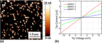
Vertically aligned, untangled planarized arrays of multiwall carbon nanotubes (MWNTs) with Ohmic back contacts were grown in nanopore templates on arbitrary substrates. The templates were prepared by sputter depositing Nd-doped Al films onto W-coated substrates, followed by anodization to form an aluminum oxide nanopore array. The W underlayer helps eliminate the aluminum oxide barrier that typically occurs at the nanopore bottoms by instead forming a thin WO3 layer. The WO3 can be selectively etched to enable electrodeposition of Co catalysts with control over the Co site density. This led to control of the site density of MWNTs grown by thermal chemical vapor deposition, with W also serving as a back electrical contact. Ohmic contact to MWNTs was confirmed, even following ultrasonic cutting of the entire array to a uniform height.

Type
Articles
Copyright
Copyright © Materials Research Society 2015 

Access options

Get access to the full version of this content by using one of the access options below. (Log in options will check for institutional or personal access. Content may require purchase if you do not have access.)

References

REFERENCES

Saito, Y. and Uemura, S.: Field emission from carbon nanotubes and its application to electron sources. Carbon 38, 169182 (2000).Google Scholar
Sotiropoulou, S. and Chaniotakis, N.A.: Carbon nanotube array-based biosensor. Anal. Bioanal. Chem. 375, 103105 (2003).Google Scholar
Liu, J., Jiang, D., Fu, Y., and Wang, T.: Carbon nanotubes for electronics manufacturing and packaging: From growth to integration. Adv. Manuf. 1, 1327 (2013).Google Scholar
Fan, S., Chapline, M.G., Franklin, N.R., Tombler, T.W., Cassell, A.M., and Dai, H.: Self-oriented regular arrays of carbon nanotubes and their field emission properties. Science 283, 512514 (1999).CrossRefGoogle ScholarPubMed
Ren, Z.F., Huang, Z.P., Xu, J.W., Wang, J.H., Bush, P., Siegal, M.P., and Provencio, P.: Synthesis of large arrays of well-aligned carbon nanotubes on glass. Science 282, 11051107 (1998).Google Scholar
Jeong, S-H., Lee, O-J., Lee, K-H., Oh, S.H., and Park, C-G.: Preparation of aligned carbon nanotubes with prescribed dimensions: Template synthesis and sonication cutting approach. Chem. Mater. 14, 18591862 (2002).CrossRefGoogle Scholar
Li, J., Papadopoulos, C., Xu, J.M., and Moskovits, M.: Highly-ordered carbon nanotube arrays for electronics applications. Appl. Phys. Lett. 75, 367369 (1999).Google Scholar
Suh, J.S. and Lee, J.S.: Highly ordered two-dimensional carbon nanotube arrays. Appl. Phys. Lett. 75, 20472049 (1999).Google Scholar
Jeong, S-H., Hwang, H.Y., Lee, K.H., and Jeong, Y.: Template-based carbon nanotubes and their application to a field emitter. Appl. Phys. Lett. 78, 20522054 (2001).Google Scholar
Jeong, S-H., Lee, O-J., Lee, K-H., Oh, S-H., and Park, C-G.: Packing density control of aligned carbon nanotubes. Chem. Mater. 14, 40034005 (2002).Google Scholar
Sklar, G.P., Paramguru, K., Misra, M., and LaCombe, J.C.: Pulsed electrodeposition into AAO templates for CVD growth of carbon nanotube arrays. Nanotechnol. 16, 12651271 (2005).CrossRefGoogle Scholar
Siegal, M.P., Overmyer, D.L., and Kaatz, F.H.: Controlling the site density of multiwall carbon nanotubes via growth conditions. Appl. Phys. Lett. 84, 51565158 (2004).Google Scholar
Oh, J. and Thompson, C.V.: Selective barrier perforation in porous alumina anodized on substrates. Adv. Mater. 20, 13681372 (2008).Google Scholar
Jeong, S-H. and Lee, K-H.: Fabrication of the aligned and patterned carbon nanotube field emitters using the anodic aluminum oxide nano-template on a Si wafer. Synth. Met. 139, 385390 (2003).CrossRefGoogle Scholar
Limmer, S.J., Yelton, W.G., Siegal, M.P., Lensch-Falk, J.L., Pillars, J., and Medlin, D.L.: Electrochemical deposition of Bi2(Te,Se)3 nanowire arrays on Si. J. Electrochem. Soc. 159, D235D239 (2012).Google Scholar
Siegal, M.P., Overmyer, D.L., and Provencio, P.P.: Precise control of multiwall carbon nanotube diameters using thermal chemical vapor deposition. Appl. Phys. Lett. 80, 21712173 (2002).Google Scholar
Siegal, M.P., Overmyer, D.L., Provencio, P.P., and Tallant, D.R.: Linear behavior of carbon nanotube diameters with growth temperature. J. Phys. Chem. C 114, 1486414867 (2010).Google Scholar
Horcas, I., Fernández, R., Gómez-Rodríguez, J.M., Colchero, J., Gómez-Herrero, J., and Baro, A.M.: WSXM: A software for scanning probe microscopy and a tool for nanotechnology. Rev. Sci. Instrum. 78, 013705 (2007).Google Scholar
Chen, P-L., Chang, J-K., Kuo, C-T., and Pan, F-M.: Field emission of carbon nanotubes on anodic aluminum oxide template with controlled tube density. Appl. Phys. Lett. 86, 123111 (2005).CrossRefGoogle Scholar
Lee, J.S., Gu, G.H., Kim, H., Jeong, K.S., Bae, J., and Suh, J.S.: Growth of carbon nanotubes on anodic aluminum oxide templates: Fabrication of a tube-in-tube and linearly joined tube. Chem. Mater. 13, 23872391 (2001).Google Scholar
Dresselhaus, M.S. and Eklund, P.C.: Phonons in carbon nanotubes. Adv. Phys. 49, 705814 (2000).Google Scholar
Kang, H.S., Yoon, H.J., Kim, C.O., Hong, J.P., Han, I.T., Cha, S.N., Song, B.K., Jung, J.E., Lee, N.S., and Kim, J.M.: Low temperature growth of multi-wall carbon nanotubes assisted by mesh potential using a modified plasma enhanced chemical vapor deposition system. Chem. Phys. Lett. 349, 196200 (2001).Google Scholar
Halonen, N., Sápi, A., Nagy, L., Puskás, R., Leino, A-R., Mäklin, J., Kukkola, J., Toth, G., Wu, M.C., Liao, H.C., Su, W.F., Shchukarev, A., Mikkola, J.P., Kukovecz, A., Konya, Z., and Kordas, K.: Low-temperature growth of multi-walled carbon nanotubes by thermal CVD. Phys. Status Solidi B 248, 25002503 (2011).CrossRefGoogle Scholar
Joon Yoon, Y., Cheol Bae, J., Koo Baik, H., Cho, S., Lee, S-J., Moon Song, K., and Myung, N.S.: Growth control of single and multi-walled carbon nanotubes by thin film catalyst. Chem. Phys. Lett. 366, 109114 (2002).CrossRefGoogle Scholar
Chen, M., Chen, C-M., and Chen, C-F.: Preparation of high yield multi-walled carbon nanotubes by microwave plasma chemical vapor deposition at low temperature. J. Mater. Sci. 37, 35613567 (2002).CrossRefGoogle Scholar
Mattia, D., Rossi, M.P., Kim, B.M., Korneva, G., Bau, H.H., and Gogotsi, Y.: Effect of graphitization on the wettability and electrical conductivity of CVD-carbon nanotubes and films. J. Phys. Chem. B 110, 98509855 (2006).CrossRefGoogle ScholarPubMed
Huang, W., Wang, Y., Luo, G., and Wei, F.: 99.9% purity multi-walled carbon nanotubes by vacuum high-temperature annealing. Carbon 41, 25852590 (2003).Google Scholar
Liang, Y., Zhen, C., Zou, D., and Xu, D.: Preparation of free-standing nanowire arrays on conductive substrates. J. Am. Chem. Soc. 126, 1633816339 (2004).Google Scholar
Limmer, S.J., Yelton, W.G., Erickson, K.J., Medlin, D.L., and Siegal, M.P.: Recrystallized arrays of bismuth nanowires with trigonal orientation. Nano Lett. 14, 19271931 (2014).CrossRefGoogle ScholarPubMed
Collins, P.G., Arnold, M.S., and Avouris, P.: Engineering carbon nanotubes and nanotube circuits using electrical breakdown. Science 292, 706709 (2001).Google Scholar