Hostname: page-component-745bb68f8f-cphqk Total loading time: 0 Render date: 2025-01-25T00:49:26.506Z Has data issue: false hasContentIssue false

Noncontact, in-line measurement of boron concentration from ultrathin boron-doped epitaxial Si1–xGex layers on Si(100) by multiwavelength micro-Raman spectroscopy

Published online by Cambridge University Press:  09 March 2011

Yu Fen Tzeng
Affiliation:
Taiwan Semiconductor Manufacturing Company, Ltd., Hsinchu, Taiwan 300-77, Republic of China
Scott Ku
Affiliation:
Taiwan Semiconductor Manufacturing Company, Ltd., Hsinchu, Taiwan 300-77, Republic of China
Stock Chang
Affiliation:
Taiwan Semiconductor Manufacturing Company, Ltd., Hsinchu, Taiwan 300-77, Republic of China
Chi Ming Yang
Affiliation:
Taiwan Semiconductor Manufacturing Company, Ltd., Hsinchu, Taiwan 300-77, Republic of China
Chyi Shieng Chern
Affiliation:
Taiwan Semiconductor Manufacturing Company, Ltd., Hsinchu, Taiwan 300-77, Republic of China
John Lin
Affiliation:
Taiwan Semiconductor Manufacturing Company, Ltd., Hsinchu, Taiwan 300-77, Republic of China
Noriyuki Hasuike
Affiliation:
Kyoto Institute of Technology, Matsugasaki, Kyoto 606-8585, Japan
Hiroshi Harima
Affiliation:
Kyoto Institute of Technology, Matsugasaki, Kyoto 606-8585, Japan
Takeshi Ueda
Affiliation:
WaferMasters, Inc., San Jose, California 95112
Toshikazu Ishigaki
Affiliation:
WaferMasters, Inc., San Jose, California 95112
Kitaek Kang
Affiliation:
WaferMasters, Inc., San Jose, California 95112
Woo Sik Yoo*
Affiliation:
WaferMasters, Inc., San Jose, California 95112
*
a)Address all correspondence to this author. e-mail: [email protected]
Get access

Abstract

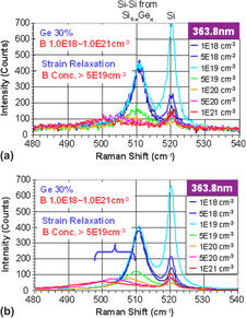
The possibility and suitability of micro-Raman spectroscopy as a noncontact, in-line measurement technique for boron (B) concentration in ultrathin (20~35 nm thick) Si1–xGex layers epitaxially grown on 300 mm diameter p-Si(100) wafers, by ultrahigh vacuum chemical vapor deposition, was investigated. Raman spectra from Si1–xGex/Si(100) wafers were measured under 363.8, 457.9, 488.0, and 514.5 nm excitation. Strong correlation was found between B content and characteristics of the Si–Si Raman peak from the Si1–xGex films. As B concentration increased from undoped to 9.1 × 10²⁰ atoms/cm3, the Si–Si Raman peak broadened and the peak height became smaller for a given Ge content. The B concentration in Si1–xGex film estimated from Raman measurement was in good agreement with secondary ion mass spectroscopy analysis results. Boron concentration as low as 8.7 × 10¹⁷ atoms/cm3 can be detected by Raman spectroscopy, which is ~30 times more sensitive than the detection limit (2.7 × 10¹⁹ atoms/cm3) of high-resolution x-ray diffraction.

Type
Articles
Copyright
Copyright © Materials Research Society 2011

Access options

Get access to the full version of this content by using one of the access options below. (Log in options will check for institutional or personal access. Content may require purchase if you do not have access.)

References

REFERENCES

1.Hikavyy, A., Nguyen, N.D., Loo, R., Ryan, P., Wormington, M., and Hopkins, J.: In-line characterization of pMOS devices with embedded SiGe and hetero bipolar transistor base layers by high-resolution x-ray diffraction, in 4th International SiGe Technology and Device Meeting (ISTDM, Hsinchu, Taiwan, May, 2008), Mon-P105.Google Scholar
2.Khater, M., Adam, T., Rieh, J.S., Schonenberg, K., Pagette, F., Stein, K., Jeng, S.J., Ahlgren, D., and Freeman, G.: Pushing the performance limits of SiGe HBT technology. ECS Transactions 3(7), 341 (2006).CrossRefGoogle Scholar
3.Zhao, L., Zuo, Y., Cheng, B., Yu, J., and Wang, Q.: Comparison between double crystals x-ray diffraction and micro-Raman measurement on composition determination of high Ge content Si1– xGex layer epitaxied on Si substrate. J. Mater. Sci. Technol. 22(5), 651 (2006).Google Scholar
4.Yoo, W.S., Ueda, T., Ishigaki, T., and Kang, K.: Non-contact, non-destructive characterization of Ge content and SiGe layer thickness using multi-wavelength Raman spectroscopy, in Proc. 17th IEEE Int. Conf. on Advanced Thermal Processing of Semiconductors (RTP 2009, Albany, NY, September, 2009), p. 169.Google Scholar
5.Yoo, W.S., Ueda, T., and Kang, K.: Characterization of uni-axially stressed Si and Ge concentration in Si1– xGe x using polychromator-based multi-wavelength Raman spectroscopy, Ext. Abs., 9th International Workshop on Junction Technology (IWJT 2009, Kyoto, Japan, June, 2009), p. 79.Google Scholar
6.Yoo, W.S., Ueda, T., Ishigaki, T., and Kang, K.: Non-destructive characterization of Ge content and Ge depth profile variations in Si1– xGex/Si by multi-wavelength Raman spectroscopy. ECS Transactions 28(1), 253 (2010).CrossRefGoogle Scholar
7.Tzeng, Y.F., Ku, S., Chang, S., Yang, C.M., Chern, C.S., Lin, J., Hasuike, N., Harima, H., Ueda, T., Ishigaki, T., Kang, K., and Yoo, W.S.: Non-contact in-line monitoring of Ge content and thickness variations of epitaxial Si1– xGex layers on Si(100) using polychromator-based multi-wavelength micro Raman spectroscopy. Appl. Phys. Exp. 3, 106601 (2010).CrossRefGoogle Scholar
8.De Wolf, I.: Raman spectroscopy: About chips and stress. Spectrosc. Eur. 15(2), 6 (2003).Google Scholar
9.Harima, H., Nakashima, S., Carulli, J.M., Beetz, C.P. Jr., and Yoo, W.S.: Characterization of 3C–SiC epitaxial layers on TiC(111) by Raman scattering. Jpn. J. Appl. Phys. 36, 5525 (1997).CrossRefGoogle Scholar
10.Nakashima, S., Mizoguchi, K., Inoue, Y., Miyauchi, M., Mitsuishi, A., Nishimura, T., and Akasaka, Y.: Raman image measurements of laser-recrystallized polycrystalline Si films by a scanning Raman microprobe. Jpn. J. Appl. Phys. Lett. 25, L222 (1986).CrossRefGoogle Scholar
11.Yoo, W.S., Kang, K., Ueda, T., and Ishigaki, T.: Design of multi-wavelength micro Raman spectroscopy system and its semiconductor stress depth profiling applications. Appl. Phys. Exp. 2, 116502 (2009).CrossRefGoogle Scholar
12.Yoo, W.S., Ueda, T., and Kang, K.: Stress depth profiling of silicon from nickel/silicon interface before and after silicide formation using polychromator-based multi-wavelength Raman spectroscopy, Ext. Absts., Int. Conf. on Solid State Devices and Materials,Tsukuba, Japan, September, 2009), p. 376.CrossRefGoogle Scholar
13.Alonso, M.I. and Winer, K.: Raman spectra of c-Si1- x Gex alloys. Phys. Rev. B 39(14), 10056 (1989).CrossRefGoogle Scholar
14.Pérez-Rodríguez, A., Romano-Rodríguez, A., Cabezas, R., Morante, J.R., Jawhari, T., and Hunt, C.E.: Effect of stress and composition on the Raman spectra of etch-stop SiGeB layers. J. Appl. Phys. 80(10), 5736 (1996).CrossRefGoogle Scholar
15.Yoo, W.S., Ueda, T., Ishigaki, T., and Kang, K.: Non-contact and non-destructive measurement of Ge and B content in Si1– xGe x/Si using very high resolution multi-wavelength Raman spectroscopy, ECS Transactions, 33(6), 877 (2010).CrossRefGoogle Scholar
16.Sze, S.M.: Physics of Semiconductor Devices, 2nd ed. (John Wiley & Sons, Inc., New York, 1981), Appendix F and H.Google Scholar
17.Dismukes, J.P., Ekstrom, L., Steigmeier, E.F., Kudman, I., and Beers, D.S.: Thermal and electrical properties of heavily doped Ge–Si alloys up to 1300 °K. J. Appl. Phys. 35, 2899 (1964).CrossRefGoogle Scholar
18.Schaffler, F.: Properties of Advanced Semiconductor Materials GaN, AlN, InN, BN, SiC, SiGe, edited by Levinshtein, M.E., Rumyantsev, S.L., and Shur, M.S. (John Wiley & Sons, Inc., New York, 2001), pp. 149188.Google Scholar