Hostname: page-component-745bb68f8f-s22k5 Total loading time: 0 Render date: 2025-01-11T06:35:23.376Z Has data issue: false hasContentIssue false

Nanoindentation cracking in gallium arsenide: Part II. TEM investigation

Published online by Cambridge University Press:  22 October 2013
Cédric Pouvreau
Affiliation:
Empa, Swiss Laboratories for Materials Science and Technology, Laboratory for Advanced Materials Processing, 3602 Thun, Switzerland; and Ecole Polytechnique Fédérale de Lausanne (EPFL), Laboratory for Mechanical Systems Design, CH-1015 Lausanne, Switzerland
Kilian Wasmer*
Affiliation:
Empa, Swiss Laboratories for Materials Science and Technology, Laboratory for Advanced Materials Processing, 3602 Thun, Switzerland
Haïcha Hessler-Wyser
Affiliation:
Ecole Polytechnique Fédérale de Lausanne (EPFL), Laboratory for Mechanical Systems Design, CH-1015 Lausanne, Switzerland
Jean-Daniel Ganière
Affiliation:
Empa, Swiss Laboratories for Materials Science and Technology, Laboratory for Advanced Materials Processing, 3602 Thun, Switzerland
Jean-Marc Breguet
Affiliation:
Ecole Polytechnique Fédérale de Lausanne (EPFL), Laboratory for Mechanical Systems Design, CH-1015 Lausanne, Switzerland
Johann Michler
Affiliation:
Empa, Swiss Laboratories for Materials Science and Technology, Laboratory for Mechanics of Materials and Nanostructures, 3602 Thun, Switzerland
Daniel Schulz
Affiliation:
Department Advanced Technologies, Bookham AG, CH-8045 Zürich, Switzerland
Jacques Henri Giovanola
Affiliation:
Ecole Polytechnique Fédérale de Lausanne (EPFL), Laboratory for Mechanical Systems Design, CH-1015 Lausanne, Switzerland
*
a)Address all correspondence to this author. e-mail: [email protected]
Get access

Abstract

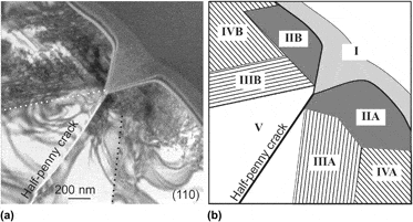
The nanoindentation fracture behavior of gallium arsenide (GaAs) is examined from two perspectives in two parent papers. In the first paper (part I), we address the morphology of the crack field induced by different types of indenters by means of in situ nanoindentation inside a scanning electron microscope (SEM) and of cleavage cross-sectioning techniques. In the present paper (part II), we investigate the early stage of crack nucleation under wedge nanoindentation through cathodoluminescence and transmission electron microscopy. We find that the apex angle of the wedge indenter influences the dislocation microstructure and, as a consequence, the mechanism of crack nucleation under nanoindentation. The formation of microtwins depends on both the orientation of the indenter with respect to the orientation of the GaAs crystal and on the apex angle of the indenter. For dicing applications of GaAs wafers, it is desirable to have an opening angle of the indenter smaller than 70° to facilitate the formation of precursor cracks.

Type
Articles
Copyright
Copyright © Materials Research Society 2013 

Access options

Get access to the full version of this content by using one of the access options below. (Log in options will check for institutional or personal access. Content may require purchase if you do not have access.)

References

REFERENCES

Wasmer, K., Pouvreau, C., Breguet, J-M., Michler, J., Schulz, D., and Giovanola, J.: Nanoindentation cracking in gallium arsenide: Part I: In situ SEM nanoindentation. J. Mater. Res. 28(20), 27852798 (2013). DOI: 10.1557/jmr.2013.252CrossRefGoogle Scholar
Wasmer, K., Ballif, C., Gassilloud, R., Pouvreau, C., Rabe, R., Michler, J., Breguet, J.M., Solletti, J-M., Karimi, A., and Schulz, D.: Aspects of cleavage fracture of brittle semiconductors from the nanometre to the centimetre scale. Adv. Eng. Mater. 7, 309 (2005).CrossRefGoogle Scholar
Wasmer, K., Ballif, C., Pouvreau, C., Schulz, D., and Michler, J.: Dicing of gallium-arsenide high performance laser diodes for industrial applications: Part I. Scratching operation. J. Mater. Process. Technol. 198, 114 (2008).CrossRefGoogle Scholar
Wasmer, K., Ballif, C., Pouvreau, C., Schulz, D., and Michler, J.: Dicing of gallium-arsenide high performance laser diodes for industrial applications: Part II. Cleavage operation. J. Mater. Process. Technol. 198, 105 (2008).CrossRefGoogle Scholar
Pouvreau, C., Wasmer, K., Giovanola, J., Breguet, J-M., Michler, J., and Karimi, A.: In-situ scanning electron microscope indentation of gallium arsenide. In 16th European Conference on Fracture (ECF16), Proceedings of the 16th European Conference of Fracture, Alexandroupolis, Greece, July 3-7, 2006 Gdoutos, E.E., ed, (Springer, New York, NY, 2006), p. 61.Google Scholar
Wasmer, K., Parlinska-Wojtan, M., Gassilloud, R., Pouvreau, C., Tharian, J., and Michler, J.: Plastic deformation modes of gallium-arsenide in nanoindentation and nanoscratching. Appl. Phys. Lett. 90, 031902 (2007).CrossRefGoogle Scholar
Parlinska-Wojtan, M., Wasmer, K., Tharian, J., and Michler, J.: Microstructural comparison of material damage in GaAs caused by Berkovich and wedge nanoindentation and nanoscratching. Scr. Mater. 59, 364 (2008).CrossRefGoogle Scholar
Wasmer, K., Parlinska-Wojtan, M., Graça, S., and Michler, J.: Sequence of deformation and cracking behaviours of gallium arsenide during nano-scratching. J. Mater. Chem. Phys. 138, 38 (2013).CrossRefGoogle Scholar
Warren, P., Pirouz, P., and Roberts, S.: Simultaneous observation of alpha and beta-dislocation movement and their effect on the fracture behaviour of GaAs. Philos. Mag. A 50, 23 (1984).Google Scholar
Androussi, Y., Vanderschaeve, G., and Lefebvre, A.: Slip and twinning in high-stress-deformed {GaAs} and the influence of doping. Philos. Mag. A 59, 1189 (1989).CrossRefGoogle Scholar
Fujita, S., Maeda, K., and Hyodo, S.: Dislocation mobility-controlled cracking in GaAs caused by constant-rate indentation. Philos. Mag. A 65, 131 (1992).CrossRefGoogle Scholar
Vanderschaeve, G.: Mechanical twinning in semiconductors. Solid State Phenom. 5960, 145 (1998).CrossRefGoogle Scholar
Bradby, J., Williams, J., Leung, J.W., Swain, M., and Munroe, P.: TEM observation of deformation microstructure under spherical indentation. Appl. Phys. Lett. 77, 3749 (2000).CrossRefGoogle Scholar
Leipner, H.S., Lorenz, D., Zeckzer, A., Lei, H., and Grau, P.: Nanoindentation pop-in effect in semiconductors. Physica B 308310, 446 (2001).CrossRefGoogle Scholar
Bradby, J.E., Williams, J.S., and Wong-Leung, J.: Mechanical deformation of InP and GaAs by spherical indentation. Appl. Phys. Lett. 78, 3235 (2001).CrossRefGoogle Scholar
Largeau, L., Patriarche, G., Le Bourhis, E., Rivière, A., and Rivière, J.: Indentation induced deformations of GaAs (011) at a high temperature. Philos. Mag. 83, 1653 (2003).CrossRefGoogle Scholar
Le Bourhis, E. and Patriarche, G.: Plastic deformation of III-V semiconductors under concentrated load. Prog. Cryst. Growth Char. Mater. 47, 1 (2003).CrossRefGoogle Scholar
Wang, S., Zhang, M., Bradby, J., and Pirouz, P.: Static microindentation and displacement sensitive indentation tests on undoped {GaAs}. In MRS Proceedings, Vol. 904, ed. J.E. Bradby, S.O. Kucheyev, E.A. Stach, M.V. Swain, (Materials Research Society, Warrendale, PA, 2005).Google Scholar
Lefebvre, A., Androussi, Y., and Vanderschaeve, G.: A TEM investigation of the dislocation rosettes around a Vickers indentation in GaAs. Phys. Status Solidi A 99, 405 (1987).CrossRefGoogle Scholar
Margevicius, R.W. and Gumbsch, P.: Influence of crack propagation direction on {110} fracture toughness of gallium arsenide. Philos. Mag. A 78, 567 (1998).CrossRefGoogle Scholar
Largeau, L. and Patriarche, G.: Subsurface deformation induced by a Vickers indenter in GaAs/AlGaAs superlattice. J. Mater. Sci. Lett. 21, 401 (2002).CrossRefGoogle Scholar
Maeda, K., Nishioka, H., Narita, N., and Fujita, S.: Brittle-to-ductile transition studied by constant-rate indentation cracking. Mater. Sci. Eng., A 176, 121 (1994).CrossRefGoogle Scholar
Giuliani, F., LLoyd, S.J., Vandeperre, L.J., and Clegg, W.J.: Deformation in GaAs under nanoindentation. EMAG, Oxford, , S.McVitie, and McCombe, D., eds., p. 123 (IOP Publishing Ltd., 2003).Google Scholar
Bradby, J., Williams, J., and Swain, M.: Pop-in events induced by spherical indentation in compound semiconductors. J. Mater. Res. 19, 380 (2004).CrossRefGoogle Scholar
Edington, J.W.: Practical Electron Microscopy in Materials Science, 2nd ed. (Van Nostrand Reinhold Company, New York, NY, 1976).Google Scholar
Hirth, J.P. and Lothe, J.: Theory of Dislocations, 2nd ed. (John Wiley and Sons, New York, NY, 1982).Google Scholar
Johnson, K.L.: Contact Mechanics, 1st ed. (Cambridge University Press, Cambridge, UK, 1985).CrossRefGoogle Scholar
Mann, A.B. and Pethica, J.B.: The role of atomic size asperities in the mechanical deformation of nanocontacts. Appl. Phys. Lett. 69, 907 (1996).CrossRefGoogle Scholar
Mann, A.B. and Pethica, J.B.: The effect of tip momentum on the contact stiffness and yielding during nanoindentation testing. Philos. Mag. A 79, 577 (1999).CrossRefGoogle Scholar
Levade, C. and Vanderschaeve, G.: Rosette microstructure in indented (001) GaAs single crystal and the alpha/beta symmetry. Phys. Status Solidi A 171, 83 (1999).3.0.CO;2-C>CrossRefGoogle Scholar
Koubaïti, S., Levade, C., Vanderschaeve, G., and Couderc, J.J.: Vickers indentation on the {001} faces of GaAs under infrared illumination and in darkness. Philos. Mag. A 80, 83 (2000).CrossRefGoogle Scholar