Hostname: page-component-745bb68f8f-5r2nc Total loading time: 0 Render date: 2025-01-11T05:42:16.809Z Has data issue: false hasContentIssue false

Influence of the deposition temperature on electronic transport and structural properties of radio frequency magnetron-sputtered Zn1-xMgxO:Al and ZnO:Al films

Published online by Cambridge University Press:  04 May 2012

André Bikowski*
Affiliation:
Department of Solar Fuels and Energy Storage Materials, Helmholtz-Zentrum Berlin für Materialien und Energie GmbH, Hahn-Meitner-Platz 1, D-14109 Berlin, Germany
Klaus Ellmer
Affiliation:
Department of Solar Fuels and Energy Storage Materials, Helmholtz-Zentrum Berlin für Materialien und Energie GmbH, Hahn-Meitner-Platz 1, D-14109 Berlin, Germany
*
a)Address all correspondence to this author. e-mail: [email protected]
Get access

Abstract

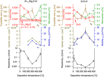
ZnO:Al and Zn1-xMgxO:Al films have been deposited by magnetron sputtering from ceramic targets at substrate temperatures from room temperature to 500 °C. We studied the relation between the electronic transport and the structural properties as a function of the deposition temperature. Films with the lowest resistivity (7·10−4 Ω cm for ZnO:Al and 3.6·10−3 Ω cm for Zn1-xMgxO:Al) can be prepared for deposition temperatures around 300 °C. This optimum is accompanied by the highest carrier concentration and the highest Hall mobility. Changes in crystalline quality and free carrier concentration are explained as a result of a bombardment of the films by high energetic negative oxygen ions during growth and by phase segregation for higher deposition temperatures. The dependence of the Hall mobility on the carrier concentration can be explained by grain barrier scattering for n <≈ 5·1020 cm−3 and by ionized impurity scattering for n >≈ 5·1020 cm−3. From the fit of the μ(n) dependence for both materials a trap density at grain boundaries of Nt ≈ 2.3·1013 cm−2 was determined.

Type
Articles
Copyright
Copyright © Materials Research Society 2012

Access options

Get access to the full version of this content by using one of the access options below. (Log in options will check for institutional or personal access. Content may require purchase if you do not have access.)

References

REFERENCES

1.Ginley, D., Hosono, H., and Paine, D., eds: Handbook of Transparent Conductors (Springer, New York, 2010).Google Scholar
2.Ellmer, K. and Mientus, R.: Carrier transport in polycrystalline transparent conductive oxides: A comparative study of zinc oxide and indium oxide. Thin Solid Films 516, 4620 (2008).CrossRefGoogle Scholar
3.Jackson, P., Hariskos, D., Lotter, E., Paetel, S., Wuerz, R., Menner, R., Wischmann, W., and Powalla, M.: New world record efficiency for Cu(In, Ga)Se(2) thin-film solar cells beyond 20%. Prog. Photovoltaics 19, 894 (2011).CrossRefGoogle Scholar
4.Siebentritt, S. and Rau, U.: Cu-Chalcopyrites—Unique materials for thin-film solar cells, In Wide-Gap Chalcopyrites, Siebentritt, S. and Rau, U., eds; Springer, Berlin, 2006; p. 1.CrossRefGoogle Scholar
5.Baruch, P., Devos, A., Landsberg, P.T., and Parrott, J.E.: On some thermodynamic aspects of photovoltaic solar-energy conversion. Sol. Energy Mater. Sol. Cells 36, 201 (1995).CrossRefGoogle Scholar
6.Siebentritt, S.: Wide gap chalcopyrites: Material properties and solar cells. Thin Solid Films 403, 1 (2002).CrossRefGoogle Scholar
7.Rau, U. and Turcu, M.: Role of surface band gap widening in Cu(In, Ga)(Se, S)2 thin-films for the photovoltaic performance of ZnO/CdS/Cu(In, Ga)(Se, S)2 heterojunction solar cells, in Compound Semiconductor Photovoltaics, edited by Noufi, R., Shafarman, W.N., Cahen, D., and Stolt, L. (Mater. Res. Soc. Symp. Proc. 763, Warrendale, PA, 2003) B8.8, p. 335.Google Scholar
8.Yamada, A., Matsubara, K., Sakurai, K., Ishizuka, S., Tampo, H., Fons, P.J., Iwata, K., and Niki, S.: Effect of band offset on the open circuit voltage of heterojunction CuIn1-xGaxSe2 solar cells. Appl. Phys. Lett. 85, 5607 (2004).CrossRefGoogle Scholar
9.Minemoto, T., Negami, T., Nishiwaki, S., Takakura, H., and Hamakawa, Y.: Preparation of Zn1-xMgxO films by radio frequency magnetron sputtering. Thin Solid Films 372, 173 (2000).CrossRefGoogle Scholar
10.Park, W.I., Yi, G.C., and Jang, H.M.: Metalorganic vapor-phase epitaxial growth and photoluminescent properties of Zn1-xMgxO(0 ≤ x ≤ 0.49) thin films. Appl. Phys. Lett. 79, 2022 (2001).CrossRefGoogle Scholar
11.Rodriguez-Carvajal, J.: FULLPROF: A Program for Rietveld Refinement and Pattern Matching Analysis, in Abstracts of the Satellite Meeting on Powder Diffraction of the XV Congress of the IUCr (Toulouse, France, 1990) p. 127.Google Scholar
12.Scherrer, P.: Determination of size and structure of colloidal particles by x-ray diffraction. Gött. Nachr 2, 98 (1918).Google Scholar
13.Keijser, T.D., Langford, J., Mittemeijer, E., and Vogels, A.: Use of the Voigt function in a single-line method for the analysis of x-ray diffraction line broadening. J. Appl. Crystallogr. 15, 308 (1982).CrossRefGoogle Scholar
14.Minami, T., Miyata, T., Yamamoto, T., and Toda, H.: Origin of electrical property distribution on the surface of ZnO: Al films prepared by magnetron sputtering. J. Vac. Sci. Technol. A 18, 1584 (2000).CrossRefGoogle Scholar
15.Dinnebier, R. and Billinge, S.: Principles of powder diffraction, in Powder Diffraction Theory and Practice, edited by Dinnebier, R. and Billinge, S. (The Royal Society of Chemistry, Cambridge, 2008), p. 19.CrossRefGoogle Scholar
16.Chen, M., Pei, Z.L., Wang, X., Sun, C., and Wen, L.S.: Dependence of structural, electrical, and optical properties of ZnO: Al films on substrate temperature. J. Mater. Res. 16, 2118 (2001).CrossRefGoogle Scholar
17.Szyszka, B.: Transparent and conductive aluminum-doped zinc oxide films prepared by mid-frequency reactive magnetron sputtering. Thin Solid Films 351, 164 (1999).CrossRefGoogle Scholar
18.Cebulla, R., Wendt, R., and Ellmer, K.: Al-doped zinc oxide films deposited by simultaneous RF and dc excitation of a magnetron plasma: Relationships between plasma parameters and structural and electrical film properties. J. Appl. Phys. 83, 1087 (1998).CrossRefGoogle Scholar
19.Pies, W. and Weiss, A.: b108, II.1.1 Simple oxides, in Landolt-Börnstein - Group III: Crystal and Solid State Physics, Numerical Data and Functional Relationships in Science and Technology, edited by Hellwege, K. and Hellwege, A. (Springer, Berlin, 1975) p. 40.Google Scholar
20.Ellmer, K.: Electrical properties, in Transparent Conductive Zinc Oxide: Basics and Applications in Thin Film Solar Cells, edited by Ellmer, K., Klein, A., and Rech, B. (Springer, Berlin, 2008) p. 35.CrossRefGoogle Scholar
21.Ellmer, K. and Welzel, T.: Reactive magnetron sputtering of transparent conductive oxide thin films: Role of energetic particle (ion) bombardment. J. Mater. Res. 27(5), 765 (2012).CrossRefGoogle Scholar
22.Windischmann, H.: Intrinsic stress in sputter-deposited thin-films. Crit. Rev. Solid State Mater Sci. 17, 547 (1992).CrossRefGoogle Scholar
23.Janotti, A. and Van de Walle, C.G.: Fundamentals of zinc oxide as a semiconductor. Rep. Prog. Phys. 72, 126501 (2009).CrossRefGoogle Scholar
24.Shirouzu, K., Ohkusa, T., Hotta, M., Enomoto, N., and Hojo, J.: Distribution and solubility limit of Al in Al2O3-doped ZnO sintered body. J. Ceram. Soc. Jpn. 115, 254 (2007).CrossRefGoogle Scholar
25.Cornelius, S., Vinnichenko, M., Shevchenko, N., Rogozin, A., Kolitsch, A., and Moller, W.: Achieving high free electron mobility in ZnO: Al thin films grown by reactive pulsed magnetron sputtering. Appl. Phys. Lett. 94, 042103 (2009).CrossRefGoogle Scholar
26.Sieber, I., Wanderka, N., Urban, I., Dorfel, I., Schierhorn, E., Fenske, F., and Fuhs, W.: Electron microscopic characterization of reactively sputtered ZnO films with different Al-doping levels. Thin Solid Films 330, 108 (1998).CrossRefGoogle Scholar
27.Han, J.P., Mantas, P.Q., and Senos, A.M.R.: Densification and grain growth of Al-doped ZnO. J. Mater. Res. 16, 459 (2001).CrossRefGoogle Scholar
28.Welzel, T., Dunger, T., Liebig, B., and Richter, F.: Determination of energy modulations of negative oxygen ions during pulsed magnetron sputtering of magnesium oxide. Plasma Sources Sci. Technol. 20, 035020 (2011).CrossRefGoogle Scholar
29.Welzel, T., Kleinhempel, R., Dunger, T., and Richter, F.: Ion energy distributions in magnetron sputtering of zinc aluminium oxide. Plasma Process. Polym. 6, S331 (2009).CrossRefGoogle Scholar
30.Depla, D., Heirwegh, S., Mahieu, S., Haemers, J., and De Gryse, R.: Understanding the discharge voltage behavior during reactive sputtering of oxides. J. Appl. Phys. 101, 013301 (2007).CrossRefGoogle Scholar
31.Mahieu, S. and Depla, D.: Correlation between electron and negative O- ion emission during reactive sputtering of oxides. Appl. Phys. Lett. 90, 121117 (2007).CrossRefGoogle Scholar
32.Ohtomo, A., Kawasaki, M., Koida, T., Masubuchi, K., Koinuma, H., Sakurai, Y., Yoshida, Y., Yasuda, T., and Segawa, Y.: MgxZn1-xO as a II-VI wide-gap semiconductor alloy. Appl. Phys. Lett. 72, 2466 (1998).CrossRefGoogle Scholar
33.Wu, C.X., Lu, Y.M., Shen, D.Z., and Fan, X.W.: Effect of Mg content on the structural and optical properties of Mg (x) Zn(1-x) O alloys. Chin. Sci. Bull. 55, 90 (2010).CrossRefGoogle Scholar
34.Lide, D., ed: Ionic Radii in Crystals, in CRC Handbook of Chemistry and Physics (CRC Press, Boca Raton, 2008) p. 12.11.Google Scholar
35.Leineweber, A. and Mittemeijer, E.J.: Anisotropic strain-like line broadening due to composition variations. Adv. X-Ray Anal. 46, 43 (2003).Google Scholar
36.Ellmer, K.: Resistivity of polycrystalline zinc oxide films: Current status and physical limit. J. Phys. D: Appl. Phys. 34, 3097 (2001).CrossRefGoogle Scholar
37.Masetti, G., Severi, M., and Solmi, S.: Modeling of carrier mobility against carrier concentration in arsenic-doped, phosphorus-doped, and boron-doped silicon. IEEE Trans. Electron. Dev. 30, 764 (1983).CrossRefGoogle Scholar
38.Seto, J.Y.W.: Electrical properties of polycrystalline silicon films. J. Appl. Phys. 46, 5247 (1975).CrossRefGoogle Scholar
39.Sondheimer, E.H.: The mean free path of electrons in metals. Adv. Phys. 1, 1 (1952).CrossRefGoogle Scholar
40.Chang, J.F. and Hon, M.H.: The effect of deposition temperature on the properties of Al-doped zinc oxide thin films. Thin Solid Films 386, 79 (2001).CrossRefGoogle Scholar
41.Chen, M., Pei, Z.L., Wang, X., Yu, Y.H., Liu, X.H., Sun, C., and Wen, L.S.: Intrinsic limit of electrical properties of transparent conductive oxide films. J. Phys. D: Appl. Phys. 33, 2538 (2000).CrossRefGoogle Scholar
42.Lipperheide, R., Weis, T., and Wille, U.: Generalized Drude model: Unification of ballistic and diffusive electron transport. J. Phys. Condens. Matter 13, 3347 (2001).CrossRefGoogle Scholar
43.Nordheim, L.: Electron theory of metals. II. Annalen der Physik 401, 641 (1931).CrossRefGoogle Scholar
44.Seager, C.H.: Grain-boundaries in polycrystalline silicon. Annu. Rev. Mater. Sci. 15, 271 (1985).CrossRefGoogle Scholar
45.Steinhauser, J., Fay, S., Oliveira, N., Vallat-Sauvain, E., Zimin, D., Kroll, U., and Ballif, C.: Electrical transport in boron-doped polycrystalline zinc oxide thin films. Phys. Status Solidi A 205, 1983 (2008).CrossRefGoogle Scholar
46.Alcock, C.B., Itkin, V.P., and Horrigan, M.K.: Vapor-pressure equations for the metallic elements—298-2500-K. Can. Metall. Q. 23, 309 (1984).CrossRefGoogle Scholar
47.Liley, P., Reid, R., and Buck, E.: Physical and chemical data, in CRC Handbook of Chemistry and Physics, edited by Weast, R. and Astle, M. (CRC Press, Inc., Florida, 1981/1982) p, 3.147.Google Scholar
48.Suga, T., Kameyama, S., Yoshioka, S., Yamamoto, T., Tanaka, I., and Mizoguchi, T.: Characterization of nanotextured AIN thin films by x-ray absorption near-edge structures. Appl. Phys. Lett. 86, 163113 (2005).CrossRefGoogle Scholar
49.Kröger, F.: The Chemistry of Imperfect Crystals (North-Holland Publishing Company, New York, 1974).Google Scholar
50.Zhang, S.B., Wei, S.H., and Zunger, A.: Intrinsic n-type versus p-type doping asymmetry and the defect physics of ZnO. Phys. Rev. B 63, 075205 (2001).CrossRefGoogle Scholar
51.Sun, Y.M. and Wang, H.Z.: The electronic properties of native interstitials in ZnO. Physica B 325, 157 (2003).CrossRefGoogle Scholar
52.Erhart, P., Albe, K., and Klein, A.: First-principles study of intrinsic point defects in ZnO: Role of band structure, volume relaxation, and finite-size effects. Phys. Rev. B 73, 205203 (2006).CrossRefGoogle Scholar
53.Roberts, N., Wang, R.P., Sleight, A.W., and Warren, W.W.: Al-27 Ga. impurity nuclear magnetic resonance ZnO: Al ZnO: Ga. Phys. Rev. B 57, 5734 (1998).CrossRefGoogle Scholar