Hostname: page-component-cd9895bd7-7cvxr Total loading time: 0 Render date: 2024-12-24T01:22:06.440Z Has data issue: false hasContentIssue false

Heat transport through interfaces with and without misfit dislocation arrays

Published online by Cambridge University Press:  15 October 2012

Anja Hanisch-Blicharski*
Affiliation:
Faculty of Physics and Center for Nanointegration Duisburg-Essen (CENIDE), University of Duisburg-Essen, 47057 Duisburg, Germany
Boris Krenzer
Affiliation:
Faculty of Physics and Center for Nanointegration Duisburg-Essen (CENIDE), University of Duisburg-Essen, 47057 Duisburg, Germany
Simone Wall
Affiliation:
Faculty of Physics and Center for Nanointegration Duisburg-Essen (CENIDE), University of Duisburg-Essen, 47057 Duisburg, Germany
Annika Kalus
Affiliation:
Faculty of Physics and Center for Nanointegration Duisburg-Essen (CENIDE), University of Duisburg-Essen, 47057 Duisburg, Germany
Tim Frigge
Affiliation:
Faculty of Physics and Center for Nanointegration Duisburg-Essen (CENIDE), University of Duisburg-Essen, 47057 Duisburg, Germany
Michael Horn-von Hoegen
Affiliation:
Faculty of Physics and Center for Nanointegration Duisburg-Essen (CENIDE), University of Duisburg-Essen, 47057 Duisburg, Germany
*
a)Address all correspondence to this author. e-mail: [email protected]
Get access

Abstract

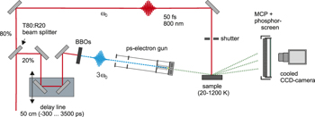
In spite of its large lattice mismatch, Bi grows epitaxially in (111) orientation and almost free of defects on Si substrates. On Si(111), the Bi film is under compressive strain of less than 2% and shows a 6–7 registry to the Si(111)-(7 × 7) substrate. On Si(001), the compressive lattice strain of 2.3% results in the formation of an array of misfit dislocations with a periodicity of 20 nm. We studied the cooling process of ultrathin bismuth films deposited on Si(111) and Si(001) substrates upon excitation with short laser pulses. With ultrafast electron diffraction, we determined the thermal boundary conductance σK from the exponential decay of the transient film temperature. Within the error bars of 7%, the experimentally determined thermal boundary conductances are the same for both substrates and thus independent of the presence of a periodic array of misfit dislocations and the different substrate orientation.

Type
Research Article
Copyright
Copyright © Materials Research Society 2012

Access options

Get access to the full version of this content by using one of the access options below. (Log in options will check for institutional or personal access. Content may require purchase if you do not have access.)

References

REFERENCES

Cahill, D.G., Ford, W.K., Goodson, K.E., Mahan, G.D., Majumdar, A., Maris, H.J., Merlin, R., and Phillpot, S.R.: Nanoscale thermal transport. J. Appl. Phys. 93, 793 (2003).CrossRefGoogle Scholar
Swartz, E.T. and Pohl, R.O.: Thermal boundary resistance. Rev. Mod. Phys. 61, 605 (1989).CrossRefGoogle Scholar
Stoner, R.J. and Maris, H.J.: Kapitza conductance and heat flow between solids at temperatures from 50 to 300 K. Phys. Rev. B: Condens. Matter 48, 16373 (1993).CrossRefGoogle ScholarPubMed
Miklowittz, J.: The Theory of Elastic Waves and Waveguides (North Holland, Amsterdam, The Netherlands, 1978).Google Scholar
Hricovini, K., Le Lay, G., Kahn, A., Taleb-Ibrahimi, A., and Bonnet, J.E.: Initial stages of Schottky-barrier formation of Bi/Si(111) and Bi/Si(100) interfaces. Appl. Surf. Sci. 5658, 259 (1992).CrossRefGoogle Scholar
Bannani, A., Bobisch, C.A., and Möller, R.: Studies on the Bi/Si(100)−(2×1) interface. Appl. Phys. Lett. 93, 032111 (2008).CrossRefGoogle Scholar
Sokolowski-Tinten, K., Blome, C., Blums, J., Cavalleri, A., Dietrich, C., Tarasevitch, A., Uschmann, I., Förster, E., Kammler, M., Horn-von Hoegen, M., and von der Linde, D.: Femtosecond x-ray measurement of coherent lattice vibrations near the Lindemann stability limit. Nature 422, 287 (2003).CrossRefGoogle ScholarPubMed
Börnstein, L.: Group III: Condensed Matter (Springer, Berlin, Germany, 2005).Google Scholar
Krenzer, B., Janzen, A., Zhou, P., von der Linde, D., and Horn-von Hoegen, M.: Thermal boundary conductance in heterostructures studied by ultrafast electron diffraction. New J. Phys. 8, 190 (2006).CrossRefGoogle Scholar
Hase, M., Mizoguchi, K., Harima, H., Nakashima, S-I., and Sakai, K.: Dynamics of coherent phonons in bismuth generated by ultrashort laser pulses. Phys. Rev. B: Condens. Matter 58, 5448 (1998).CrossRefGoogle Scholar
Krenzer, B., Hanisch, A., Duvenbeck, A., Rethfeld, B., and Horn-von Hoegen, M.: Heat transport in nanoscale heterosystems: A numerical and analytical study. J. Nanomaterials, 590609 (2008).Google Scholar
Jnawali, G., Hattab, H., Meyer zu Heringdorf, F.J., Krenzer, B., and Horn-von Hoegen, M.: Lattice-matching periodic array of misfit dislocations: Heteroepitaxy of Bi(111) on Si(001). Phys. Rev. B 76, 035337 (2007).CrossRefGoogle Scholar
Jnawali, G., Hattab, H., Krenzer, B., and Horn-von Hoegen, M.: Lattice accommodation of epitaxial Bi(111) films on Si(001) studied with SPA-LEED and AFM. Phys. Rev. B 74, 195340 (2006).CrossRefGoogle Scholar
Kammler, M. and Horn-von Hoegen, M.: Low energy electron diffraction of epitaxial growth of bismuth on Si(111). Surf. Sci. 576, 56 (2005).CrossRefGoogle Scholar
Hirahara, T., Matsuda, I., Yamazaki, S., Miyata, N., Hasegawa, S., and Nagao, T.: Large surface-state conductivity in ultrathin Bi films. Appl. Phys. Lett. 91, 202106 (2007).CrossRefGoogle Scholar
Jnawali, G., Hattab, H., Bobisch, C.A., Bernhart, A., Zubkov, E., Möller, R., and Horn-von Hoegen, M.: Nanoscale dislocation patterning in Bi(111)/Si(001) heteroepitaxy. Surf. Sci. 603, 2057 (2009).CrossRefGoogle Scholar
Kury, P., Hild, R., Thien, D., Günter, H-L., Meyer zu Heringdorf, F-J., and Horn-von Hoegen, M.: Compact and transferable threefold evaporator for molecular beam epitaxy in ultrahigh vacuum. Rev. Sci. Instrum. 76, 083906 (2005).CrossRefGoogle Scholar
Yaginuma, S., Nagao, T., Sadowski, J.T., Pucci, A., and Sakurai, T.: Surface pre-melting and surface flattening of Bi nanofilms on Si(111)-7×7. Surf. Sci. 547, L877 (2003).CrossRefGoogle Scholar
Janzen, A., Krenzer, B., Zhou, P., von der Linde, D., and Horn- von Hoegen, M.: Ultrafast electron diffraction at surfaces after laser excitation. Surf. Sci. 600, 4094 (2006).CrossRefGoogle Scholar
Ha, J.S. and Greene, E.F.: Observation of phase transitions on the (111) and (100) surfaces of Si near 1000 K with He atom diffraction. J. Chem. Phys. 91, 571 (1989).CrossRefGoogle Scholar
Stevens, R.J., Smith, A.N., and Norris, P.M.: Measurement of thermal boundary conductance of a series of metal-dielectric interfaces by the transient thermoreflectance technique. J. Heat Transfer 127, 315 (2005).CrossRefGoogle Scholar
Nabarro, F.R.N.: Theory of Crystal Dislocation (Dover, New York, 1987).Google Scholar
Gradmann, U. and Waller, G.: Periodic lattice distortions in epitaxial films of Fe(110) on W(110). Surf. Sci. 116, 539 (1982).CrossRefGoogle Scholar
Stalder, R., Sirringhaus, H., Onda, N., and von Känel, H.: Observation of misfit dislocations in epitaxial CoSi2/Si (111) layers by scanning tunneling microscopy. Appl. Phys. Lett. 59, 1960 (1991).CrossRefGoogle Scholar
Horn-von Hoegen, M., Al-Falou, A., Pietsch, H., Müller, B.H., and Henzler, M.: Formation of interfacial dislocation network in surfactant mediated growth of Ge on Si(111) investigated by SPA-LEED: Part I. Surf. Sci. 298, 29 (1993).CrossRefGoogle Scholar
Horn-von Hoegen, M., Schmidt, T., Meyer, G., Winau, D., and Riede, K.H.: Lattice accommodation of low-index planes: Ag(111) on Si(001). Phys. Rev. B: Condens. Matter 52, 10764 (1995).CrossRefGoogle Scholar
Springholz, G.: Strain contrast in scanning tunneling microscopy imaging of subsurface dislocations in lattice-mismatched heteroepitaxy. Appl. Surf. Sci. 112, 12 (1997).CrossRefGoogle Scholar
Filimonov, S.N., Cherepanov, V., Paul, N., Asaoka, H., Brona, J., and Voigtländer, B.: Dislocation networks in conventional and surfactant-mediated Ge/Si(111) epitaxy. Surf. Sci. 599, 76 (2005).CrossRefGoogle Scholar
Abramson, A.R., Tien, C-L., and Majumdar, A.: Interface and strain effects on the thermal conductivity of heterostructures: A molecular dynamics study. J. Heat Transfer 124, 963 (2002).CrossRefGoogle Scholar
Li, X., Maute, K., Dunn, M.L., and Yang, R.: Strain effects on the thermal conductivity of nanostructures. Phys. Rev. B 81, 245318 (2010).CrossRefGoogle Scholar
Hepplestone, S.P. and Srivastava, G.P.: Theory of interface scattering of phonons in superlattices. Phys. Rev. B 82, 144303 (2010).CrossRefGoogle Scholar
Lee, S.M., Cahill, D.G., and Venkatasubramanian, R.: Thermal conductivity of Si–Ge superlattices. Appl. Phys. Lett. 70, 2957 (1997).CrossRefGoogle Scholar
Hopkins, P.E., Duda, J.C., Clark, S.P., Hains, C.P., Rotter, T.J., Pinney, L.M., and Balakrishnan, G.: Effect of dislocation density on thermal boundary conductance across GaSb/GaAs interfaces. Appl. Phys. Lett. 98, 161913 (2011).CrossRefGoogle Scholar