Hostname: page-component-745bb68f8f-v2bm5 Total loading time: 0 Render date: 2025-01-10T20:57:15.289Z Has data issue: false hasContentIssue false

Electrostatic self-assembly of nanoparticles into ordered nanowire arrays

Published online by Cambridge University Press:  24 January 2011

Jun Tang
Affiliation:
Department of Applied Physics, National Technical University of Athens, 15780 Zografou, Greece
E. Verrelli
Affiliation:
Department of Applied Physics, National Technical University of Athens, 15780 Zografou, Greece
K. Giannakopoulos
Affiliation:
Institute of Materials Science, NCSR Demokritos, 15310 Aghia Paraskevi, Greece
D. Tsoukalas*
Affiliation:
Department of Applied Physics, National Technical University of Athens, 15780 Zografou, Greece; and Institute of Microelectronics, NCSR Demokritos, 15310 Aghia Paraskevi, Greece
*
a)Address all correspondence to this author. e-mail: [email protected]
Get access

Abstract

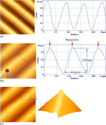
A novel nanoparticle self-assembly process is demonstrated. Nanoparticles were fabricated by a DC magnetron sputtering process. A silicon substrate was initially patterned with arrays of peak and valley photoresist structures using inexpensive patterning techniques. When the nanoparticles were deposited onto the prepatterned substrate, due to surface topography induced local increase in the electric field created by the charges on the nanoparticles, the nanoparticles were self-assembled onto the peaks of the structures and formed long nanowire arrays.

Type
Reviews
Copyright
Copyright © Materials Research Society 2011

Access options

Get access to the full version of this content by using one of the access options below. (Log in options will check for institutional or personal access. Content may require purchase if you do not have access.)

References

REFERENCES

1.Koh, S.J.: Strategies for controlled placement of nanoscale building blocks. Nanoscale Res. Lett. 2, 519 (2007).CrossRefGoogle ScholarPubMed
2.Chai, J., Wang, D., Fan, A., and Buriak, J.M.: Assembly of aligned linear metallic patterns on silicon. Nat. Nanotechnol. 2, 500 (2007).CrossRefGoogle ScholarPubMed
3.Joo, J., Moon, S., and Jacobson, J.M.: Ultrafast patterning of nanoparticles by electrostatic lithography. J. Vac. Sci. Technol., B 24, 3205 (2006).CrossRefGoogle Scholar
4.Mesquida, P. and Stemmer, A.: Attaching silica nanoparticles from suspension onto surface charge patterns generated by a conductive atomic force microscope tip. Adv. Mater. 13, 1395 (2001).3.0.CO;2-0>CrossRefGoogle Scholar
5.Barry, C.R., Steward, M.G., Lwin, N.Z., and Jacobs, H.O.: Printing nanoparticles from the liquid and gas phases using nanoxerography. Nanotechnology 14, 1057 (2003).CrossRefGoogle Scholar
6.Kim, H., Kim, J., Yang, H., Suh, J., Kim, T., Han, B., Kim, S., Kim, D.S., Pikhitsk, P.V., and Choi, M.: Parallel patterning of nanoparticles via electrodynamic focusing of charged aerosols. Nat. Nanotechnol. 1, 117 (2006).CrossRefGoogle ScholarPubMed
7.Hermanson, K.D., Lumsdon, S.O., Williams, J.P., Kaler, E.W., and Velev, O.D.: Dielectrophoretic assembly of electrically functional microwires from nanoparticle suspensions. Science 294, 1082 (2001).CrossRefGoogle ScholarPubMed
8.Huang, H., Bhadrachalam, P., Ray, V., and Koh, S.J.: Single-particle placement via self-limiting electrostatic gating. Appl. Phys. Lett. 93, 073110 (2008).CrossRefGoogle Scholar
9.Oates, T.W.H., Keller, A., Noda, S., and Facsko, S.: Self-organized metallic nanoparticle and nanowires arrays from ion-sputtered silicon templates. Appl. Phys. Lett. 93, 063106 (2008).CrossRefGoogle Scholar
10.Hsu, P.J., Wu, C.B., Yen, H.Y., Wong, S.S., Lin, W.C., and Lin, M.T.: Electronically patterning through one-dimensional nanostripes with high density of states on single crystalline Al2O3 domain. Appl. Phys. Lett. 93, 143104 (2008).CrossRefGoogle Scholar
11.Krishnan, M., Petrasek, Z., Monch, I., and Schwille, P.: Electrostatic self-assembly of charged colloids and macromolecules in fluidic nanoslit. Small 11, 1900 (2008).CrossRefGoogle Scholar
12.Kean, A.H. and Allers, L.: The analysis of coatings produced by accelerated nanoparticles, in Proceedings of the 2006 NSTI Nanotech Conference (2006).Google Scholar
13.Tang, J., Verreli, E., and Tsoukalas, D.: Assembly of charged nanoparticles using self-electrodynamic focusing. Nanotechnology 20, 36 365605 (2009).CrossRefGoogle ScholarPubMed
14.Qia, C., Chen, D.R., and Greenberg, P.: Performance study of a unipolar aerosol mini-charger for a personal nanoparticle sizer. J. Aerosol Sci. 39, 450 (2008).CrossRefGoogle Scholar
15.Aliat, A., Tsai, C-J., Hung, C-T., and Wu, J-S.: Effect of free electrons on nanoparticle charging in a negative direct current corona charger. Appl. Phys. Lett. 93, 154103 (2008).CrossRefGoogle Scholar
16.Chai, H.: A note on crack trajectory in an elastic strip bounded by rigid substrates. Int. J. Fract. 32, 211 (1987).CrossRefGoogle Scholar
17.Pease, L.F., Deshpande, P., Wang, Y., Russel, W.B., and Chou, S.Y.: Self-formation of sub-60-nm half-pitch gratings with large areas through fracturing. Nat. Nanotechnol. 2, 545 (2007).CrossRefGoogle ScholarPubMed
18.Tang, J., Kolliopoulou, S., and Tsoukalas, D.: Fabrication of gold nanoparticle lines based on fracture induced patterning. Microelectron. Eng. 86, 861 (2009).CrossRefGoogle Scholar
19.Jackson, J.D.: Classical Electrodynamics (John Wiley and Sons, New York, 1999).Google Scholar
20.Ravishankar, N., Shenoy, V.B., and Carter, C.B.: Electric field singularity assisted nanopatterning. Adv. Mater. 16, 76 (2004).CrossRefGoogle Scholar
21.Koening, G., Ong, J.R., Cortes, A.D., Moreno-Razo, J.A., de Pablo, J.J., and Abbot, N.L.: Single nanoparticle tracking reveals influence of chemical functionality of nanoparticles on local ordering of liquid crystals and nanoparticle diffusion coefficients. Nano Lett. 9, 2794 (2009).CrossRefGoogle Scholar