Hostname: page-component-586b7cd67f-dsjbd Total loading time: 0 Render date: 2024-11-29T17:06:48.673Z Has data issue: false hasContentIssue false

Electronic structure of designed [(SnSe)1+δ]m[TiSe2]2 heterostructure thin films with tunable layering sequence

Published online by Cambridge University Press:  29 April 2019
Fabian Göhler
Affiliation:
Institute of Physics, Chemnitz University of Technology, D-09126 Chemnitz, Germany
Danielle M. Hamann
Affiliation:
Department of Chemistry, University of Oregon, Eugene, Oregon 97401, USA
Niels Rösch
Affiliation:
Institute of Physics, Chemnitz University of Technology, D-09126 Chemnitz, Germany
Susanne Wolff
Affiliation:
Institute of Physics, Chemnitz University of Technology, D-09126 Chemnitz, Germany
Jacob T. Logan
Affiliation:
Department of Chemistry, University of Oregon, Eugene, Oregon 97401, USA
Robert Fischer
Affiliation:
Department of Chemistry, University of Oregon, Eugene, Oregon 97401, USA
Florian Speck
Affiliation:
Institute of Physics, Chemnitz University of Technology, D-09126 Chemnitz, Germany
David C. Johnson
Affiliation:
Department of Chemistry, University of Oregon, Eugene, Oregon 97401, USA
Thomas Seyller*
Affiliation:
Institute of Physics, Chemnitz University of Technology, D-09126 Chemnitz, Germany
*
a)Address all correspondence to this author. e-mail: [email protected]
Get access

Abstract

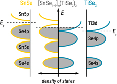
A series of ${\left\hbox[ {{{\left\hbox( {{\rm{SnSe}}} \right\hbox)}_{1 \hbox+ \delta }}} \right\hbox]_m}{\left\hbox[ {{\rm{TiS}}{{\rm{e}}_2}} \right\hbox]_2}$ heterostructure thin films built up from repeating units of m bilayers of SnSe and two layers of TiSe2 were synthesized from designed precursors. The electronic structure of the films was investigated using X-ray photoelectron spectroscopy for samples with m = 1, 2, 3, and 7 and compared to binary samples of TiSe2 and SnSe. The observed binding energies of core levels and valence bands of the heterostructures are largely independent of m. For the SnSe layers, we can observe a rigid band shift in the heterostructures compared to the binary, which can be explained by electron transfer from SnSe to TiSe2. The electronic structure of the TiSe2 layers shows a more complicated behavior, as a small shift can be observed in the valence band and Se3d spectra, but the Ti2p core level remains at a constant energy. Complementary UV photoemission spectroscopy measurements confirm a charge transfer mechanism where the SnSe layers donate electrons into empty Ti3d states at the Fermi energy.

Type
Invited Paper
Copyright
Copyright © Materials Research Society 2019 

Access options

Get access to the full version of this content by using one of the access options below. (Log in options will check for institutional or personal access. Content may require purchase if you do not have access.)

References

Geim, A.K. and Grigorieva, I.V.: Van der Waals heterostructures. Nature 499, 419 (2013).CrossRefGoogle ScholarPubMed
Ferrari, A.C., Bonaccorso, F., Fal’ko, V., Novoselov, K.S., Roche, S., Bøggild, P., Borini, S., Koppens, F.H.L., Palermo, V., Pugno, N., Garrido, J.A., Sordan, R., Bianco, A., Ballerini, L., Prato, M., Lidorikis, E., Kivioja, J., Marinelli, C., Ryhänen, T., Morpurgo, A., Coleman, J.N., Nicolosi, V., Colombo, L., Fert, A., Garcia-Hernandez, M., Bachtold, A., Schneider, G.F., Guinea, F., Dekker, C., Barbone, M., Sun, Z., Galiotis, C., Grigorenko, A.N., Konstantatos, G., Kis, A., Katsnelson, M., Vandersypen, L., Loiseau, A., Morandi, V., Neumaier, D., Treossi, E., Pellegrini, V., Polini, M., Tredicucci, A., Williams, G.M., Hong, B.H., Ahn, J-H., Kim, J.M., Zirath, H., van Wees, B.J., van der Zant, H., Occhipinti, L., Matteo, A.D., Kinloch, I.A., Seyller, T., Quesnel, E., Feng, X., Teo, K., Rupesinghe, N., Hakonen, P., Neil, S.R.T., Tannock, Q., Löfwander, T., and Kinaret, J.: Science and technology roadmap for graphene, related two-dimensional crystals, and hybrid systems. Nanoscale 7, 4598 (2015).CrossRefGoogle ScholarPubMed
Kuc, A., Heine, T., and Kis, A.: Electronic properties of transition-metal dichalcogenides. MRS Bull. 40, 577 (2015).CrossRefGoogle Scholar
Robinson, J.A.: Growing vertical in the flatland. ACS Nano 10, 42 (2016).CrossRefGoogle ScholarPubMed
Novoselov, K.S., Fal’ko, V.I., Colombo, L., Gellert, P.R., Schwab, M.G., and Kim, K.: A roadmap for graphene. Nature 490, 192 (2012).CrossRefGoogle ScholarPubMed
Dean, C.R., Young, A.F., Meric, I., Lee, C., Wang, L., Sorgenfrei, S., Watanabe, K., Taniguchi, T., Kim, P., Shepard, K.L., and Hone, J.: Boron nitride substrates for high-quality graphene electronics. Nat. Nanotechnol. 5, 722 (2010).CrossRefGoogle ScholarPubMed
Mayorov, A.S., Gorbachev, R.V., Morozov, S.V., Britnell, L., Jalil, R., Ponomarenko, L.A., Blake, P., Novoselov, K.S., Watanabe, K., Taniguchi, T., and Geim, A.K.: Micrometer-scale ballistic transport in encapsulated graphene at room temperature. Nano Lett. 11, 2396 (2011).CrossRefGoogle ScholarPubMed
Grosse, C., Alemayehu, M.B., Mogilatenko, A., Chiatti, O., Johnson, D.C., and Fischer, S.F.: Superconducting tin selenide/niobium diselenide ferecrystals. Cryst. Res. Technol. 52, 1700126 (2017).CrossRefGoogle Scholar
Kang, K., Lee, K-H., Han, Y., Gao, H., Xie, S., Muller, D.A., and Park, J.: Layer-by-layer assembly of two-dimensional materials into wafer-scale heterostructures. Nature 550, 229 (2017).CrossRefGoogle ScholarPubMed
Wiegers, G.: Misfit layer compounds: Structures and physical properties. Prog. Solid State Chem. 24, 1 (1996).CrossRefGoogle Scholar
Rouxel, J., Meerschaut, A., and Wiegers, G.: Chalcogenide misfit layer compounds. J. Alloys Compd. 229, 144 (1995).CrossRefGoogle Scholar
Merrill, D., Moore, D., Bauers, S., Falmbigl, M., and Johnson, D.: Misfit layer compounds and ferecrystals: Model systems for thermoelectric nanocomposites. Materials 8, 2000 (2015).CrossRefGoogle ScholarPubMed
Withers, F., Pozo-Zamudio, O.D., Mishchenko, A., Rooney, A.P., Gholinia, A., Watanabe, K., Taniguchi, T., Haigh, S.J., Geim, A.K., Tartakovskii, A.I., and Novoselov, K.S.: Light-emitting diodes by band-structure engineering in van der Waals heterostructures. Nat. Mater. 14, 301 (2015).CrossRefGoogle ScholarPubMed
Novoselov, K.S., Mishchenko, A., Carvalho, A., and Neto, A.H.C.: 2D materials and van der Waals heterostructures. Science 353, aac9439 (2016).CrossRefGoogle Scholar
Liu, Y., Weiss, N.O., Duan, X., Cheng, H-C., Huang, Y., and Duan, X.: Van der Waals heterostructures and devices. Nat. Rev. Mater. 1, 16042 (2016).CrossRefGoogle Scholar
Esters, M., Alemayehu, M.B., Jones, Z., Nguyen, N.T., Anderson, M.D., Grosse, C., Fischer, S.F., and Johnson, D.C.: Synthesis of inorganic structural isomers by diffusion-constrained self-assembly of designed precursors: A novel type of isomerism. Angew. Chem., Int. Ed. 54, 1130 (2015).CrossRefGoogle ScholarPubMed
Westover, R., Atkins, R.A., Falmbigl, M., Ditto, J.J., and Johnson, D.C.: Self-assembly of designed precursors: A route to crystallographically aligned new materials with controlled nanoarchitecture. J. Solid State Chem. 236, 173 (2016).CrossRefGoogle Scholar
Beekman, M., Heideman, C.L., and Johnson, D.C.: Ferecrystals: Non-epitaxial layered intergrowths. Semicond. Sci. Technol. 29, 064012 (2014).CrossRefGoogle Scholar
Wan, C., Wang, Y., Wang, N., and Koumoto, K.: Low-thermal-conductivity (MS)1+x(TiS2)2 (M = Pb, Bi, Sn) misfit layer compounds for bulk thermoelectric materials. Materials 3, 2606 (2010).CrossRefGoogle Scholar
Merrill, D.R., Moore, D.B., Ditto, J., Sutherland, D.R., Falmbigl, M., Winkler, M., Pernau, H-F., and Johnson, D.C.: The synthesis, structure, and electrical characterization of (SnSe)1.2(TiSe)2. Eur. J. Inorg. Chem. 2015, 83 (2015).CrossRefGoogle Scholar
Li, Z., Bauers, S.R., Poudel, N., Hamann, D., Wang, X., Choi, D.S., Esfarjani, K., Shi, L., Johnson, D.C., and Cronin, S.B.: Cross-plane Seebeck coefficient measurement of misfit layered compounds (SnSe)n(TiSe2)n (n = 1, 3, 4, 5). Nano Lett. 17, 1978 (2017).CrossRefGoogle Scholar
Hamann, D.M., Merrill, D.R., Bauers, S.R., Mitchson, G., Ditto, J., Rudin, S.P., and Johnson, D.C.: Long-range order in [(SnSe)1.2]1[TiSe2]1 prepared from designed precursors. Inorg. Chem. 56, 3499 (2017).CrossRefGoogle Scholar
Hamann, D.M., Lygo, A.C., Esters, M., Merrill, D.R., Ditto, J., Sutherland, D.R., Bauers, S.R., and Johnson, D.C.: Structural changes as a function of thickness in [(SnSe)1+δ]mTiSe2 heterostructures. ACS Nano 12, 1285 (2018).CrossRefGoogle Scholar
Morosan, E., Zandbergen, H.W., Dennis, B.S., Bos, J.W.G., Onose, Y., Klimczuk, T., Ramirez, A.P., Ong, N.P., and Cava, R.J.: Superconductivity in CuxTiSe2. Nat. Phys. 2, 544 (2006).CrossRefGoogle Scholar
Morosan, E., Wagner, K.E., Zhao, L.L., Hor, Y., Williams, A.J., Tao, J., Zhu, Y., and Cava, R.J.: Multiple electronic transitions and superconductivity in PdxTiSe2. Phys. Rev. B 81, 094524 (2010).CrossRefGoogle Scholar
Göhler, F., Mitchson, G., Alemayehu, M.B., Speck, F., Wanke, M., Johnson, D.C., and Seyller, T.: Charge transfer in (PbSe)1+δ(NbSe2)2 and (SnSe)1+δ(NbSe2)2 ferecrystals investigated by photoelectron spectroscopy. J. Phys.: Condens. Matter 30, 055001 (2018).Google Scholar
Johnson, D.C.: Controlled synthesis of new compounds using modulated elemental reactants. Curr. Opin. Solid State Mater. Sci. 3, 159 (1998).CrossRefGoogle Scholar
Hamann, D.M., Bardgett, D., Cordova, D.L.M., Maynard, L.A., Hadland, E.C., Lygo, A.C., Wood, S.R., Esters, M., and Johnson, D.C.: Sub-monolayer accuracy in determining the number of atoms per unit area in ultrathin films using X-ray fluorescence. Chem. Mater. 30, 6209 (2018).CrossRefGoogle Scholar
Moore, D.B., Sitts, L., Stolt, M.J., Beekman, M., and Johnson, D.C.: Characterization of nonstoichiometric Ti1+xSe2 prepared by the method of modulated elemental reactants. J. Electron. Mater. 42, 1647 (2013).CrossRefGoogle Scholar
Chen, J., Hamann, D.M., Choi, D., Poudel, N., Shen, L., Shi, L., Johnson, D.C., and Cronin, S.: Enhanced cross-plane thermoelectric transport of rotationally disordered SnSe2 via Se-vapor annealing. Nano Lett. 18, 6876 (2018).CrossRefGoogle ScholarPubMed
Makinistian, L. and Albanesi, E.A.: On the band gap location and core spectra of orthorhombic IV–VI compounds SnS and SnSe. Phys. Status Solidi B 246, 183 (2009).CrossRefGoogle Scholar
Rasch, J.C.E., Stemmler, T., Müller, B., Dudy, L., and Manzke, R.: 1T-TiSe2: Semimetal or semiconductor? Phys. Rev. Lett. 101, 237602 (2008).CrossRefGoogle ScholarPubMed
Doniach, S. and Sunjic, M.: Many-electron singularity in X-ray photoemission and X-ray line spectra from metals. J. Phys. C: Solid State Phys. 3, 285 (1970).CrossRefGoogle Scholar
Mahan, G.D.: Collective excitations in X-ray spectra of metals. Phys. Rev. B 11, 4814 (1975).CrossRefGoogle Scholar
Shkvarin, A.S., Yarmoshenko, Y.M., Skorikov, N.A., Yablonskikh, M.V., Merentsov, A.I., Shkvarina, E.G., and Titov, A.N.: Electronic structure of titanium dichalcogenides TiX2 (X = S, Se, Te). J. Exp. Theor. Phys. 114, 150 (2012).CrossRefGoogle Scholar
Shirley, D.A.: High-resolution X-ray photoemission spectrum of the valence bands of gold. Phys. Rev. B 5, 4709 (1972).CrossRefGoogle Scholar
Ohta, T., Bostwick, A., McChesney, J.L., Seyller, T., Horn, K., and Rotenberg, E.: Interlayer interaction and electronic screening in multilayer graphene investigated with angle-resolved photoemission spectroscopy. Phys. Rev. Lett. 98, 206802 (2007).CrossRefGoogle ScholarPubMed
Bostwick, A., Ohta, T., McChesney, J.L., Emtsev, K.V., Seyller, T., Horn, K., and Rotenberg, E.: Symmetry breaking in few layer graphene films. New J. Phys. 9, 385 (2007).CrossRefGoogle Scholar
Emtsev, K.V., Speck, F., Seyller, T., Ley, L., and Riley, J.D.: Interaction, growth, and ordering of epitaxial graphene on SiC{0001} surfaces: A comparative photoelectron spectroscopy study. Phys. Rev. B 77, 155303 (2008).CrossRefGoogle Scholar
Brandt, J., Kipp, L., Skibowski, M., Krasovskii, E., Schattke, W., Spiecker, E., Dieker, C., and Jäger, W.: Charge transfer in misfit layered compounds. Surf. Sci. 532, 705 (2003).CrossRefGoogle Scholar
Shalvoy, R., Fisher, G., and Stiles, P.: X-ray photoemission studies of the valence bands of nine IV–VI compounds. Phys. Rev. B 15, 2021 (1977).CrossRefGoogle Scholar
Giang, N., Xu, Q., Hor, Y.S., Williams, A.J., Dutton, S.E., Zandbergen, H.W., and Cava, R.J.: Superconductivity at 2.3 K in the misfit compound(PbSe)1.16(TiSe2)2. Phys. Rev. B 82, 024503 (2010).CrossRefGoogle Scholar
Moore, D.B., Beekman, M., Disch, S., Zschack, P., Häusler, I., Neumann, W., and Johnson, D.C.: Synthesis, structure, and properties of turbostratically disordered (PbSe)1.18(TiSe2)2. Chem. Mater. 25, 2404 (2013).CrossRefGoogle Scholar
Schröder, U.A., Petrović, M., Gerber, T., Martínez-Galera, A.J., Grånäs, E., Arman, M.A., Herbig, C., Schnadt, J., Kralj, M., Knudsen, J., and Michely, T.: Core level shifts of intercalated graphene. 2D Mater. 4, 015013 (2017).CrossRefGoogle Scholar
Esters, M.: Deposition software for the inficon IC6 deposition controller (2018). Available at: https://github.com/marcoesters/deposition_ic6 (accessed December 04, 2018).Google Scholar