Hostname: page-component-586b7cd67f-dsjbd Total loading time: 0 Render date: 2024-11-27T00:04:04.183Z Has data issue: false hasContentIssue false

Aberration-corrected self-interference of split higher order Laue zone line for measuring the z-dependent strain profile

Published online by Cambridge University Press:  16 January 2017
Mana Norouzpour*
Affiliation:
CAMTEC, MENG, University of Victoria, British Colombia V8W 2Y2, Canada
Rodney Herring
Affiliation:
CAMTEC, MENG, University of Victoria, British Colombia V8W 2Y2, Canada
*
a)Address all correspondence to this author. e-mail: [email protected]
Get access

Abstract

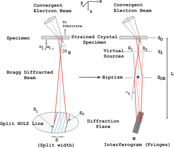
A common characteristic in semiconductor nanostructures is the lattice strain originating from the lattice mismatch between layers of different compositions. Three-dimensional strain measurement in crystals using transmission electron microscopy (TEM) techniques has been the subject of intense works for decades. This information is required for the strain-bandgap engineering being used by our current fast computers and necessary for future quantum computers. However, the missing information was the 3rd dimension that is the atomic displacement and how it changes along the electron-beam direction. The strain information along the electron-beam direction is in the phase of the diffracted beam, which has been obtained recently by the novel technique of self-interference of split higher order Laue zone line (SIS-HOLZ). SIS-HOLZ has been made possible by the correction of the beam aberrations having its analytical and experimental details reported here for the atomic displacement profile existing at the interface of a Si and Si/Si0.8Ge0.2 superlattice.

Type
Articles
Copyright
Copyright © Materials Research Society 2017 

Access options

Get access to the full version of this content by using one of the access options below. (Log in options will check for institutional or personal access. Content may require purchase if you do not have access.)

Footnotes

Contributing Editor: Thomas Walther

References

REFERENCES

Chun, M., Sun, Y., Aghoram, U., and Thompson, S.E.: Strain: A solution for higher carrier mobility in nanoscale MOSFETs. Annu. Rev. Mater. Res. 39, 203229 (2009).Google Scholar
Sun, Y., Thompson, S.E., and Nishida, T.: Strain Effect in Semiconductors: Theory and Device Applications (Springer, London, 2010); pp. 235266.Google Scholar
Deelman, P.W., Edge, L.F., and Jackson, C.A.: Metamorphic materials for quantum computing. MRS Bull. 41(03), 224230 (2016).Google Scholar
Hӱtch, M.J., Snoeck, E., and Kilaas, R.: Quantitative measurement of displacement and strain fields from hrem micrographs. Ultramicroscopy 74(3), 131146 (1998).Google Scholar
Hӱtch, M.J. and Potez, L.: Geometric phase analysis of high-resolution electron microscopy images of antiphase domains: Example Cu3Au. Philos. Mag. 76(6), 11191138 (1997).Google Scholar
Saitoh, K., Nakahara, H., and Tanaka, N.: Improvement of the precision of lattice parameter determination by nano-beam electron diffraction. Microscopy 69(5), 533539 (2013).Google Scholar
Favia, P., Gonzales, M.B., Simoen, E., Verheyen, P., Klenov, D., and Bender, H.: Nanobeam diffraction: Technique evaluation and strain measurement on complementary metal oxide semiconductor devices. J. Electrochem. Soc. 158(4), H438H446 (2011).Google Scholar
Armigliato, A., Balboni, R., Carnevale, G., Pavia, G., Piccolo, D., Frabboni, S., Benedetti, A., and Cullis, A.G.: Application of convergent beam electron diffraction to two-dimensional strain mapping in silicon devices. Appl. Phys. Lett. 82(13), 21722174 (2003).Google Scholar
Lu, Z., Pyczak, F., Krämer, S., Biermann, H., and Mughrabi, H.: Fast and reliable evaluation of lattice distortions from convergent-beam electron diffraction patterns. Philos. Mag. 83(20), 23832397 (2003).Google Scholar
Houdellier, F., Roucau, C., Clement, L., Rouvière, J., and Casanove, M.: Quantitative analysis of HOLZ line splitting in CBED patterns of epitaxially strained layers. Ultramicroscopy 106(10), 951959 (2006).Google Scholar
Saitoh, K., Yasuda, Y., Hamabe, M., and Tanaka, N.: Automated characterization of bending and expansion of a lattice of a Si substrate near a SiGe/Si interface by using split HOLZ line patterns. J. Electron Microsc. 59(10), 367378 (2010).Google Scholar
Clément, L., Pantel, R., Kwakman, L.T., and Rouvière, J.L.: Strain measurements by convergent-beam electron diffraction: The importance of stress relaxation in lamella preparations. Appl. Phys. Lett. 84(5), 651653 (2004).Google Scholar
Cooper, D., Barnes, J.P., Hartmann, J.M., Béché, A., and Rouvière, J.L.: Dark field electron holography for quantitative strain measurements with nanometer-scale spatial resolution. Appl. Phys. Lett. 95(5), 053501053503 (2009).Google Scholar
Béché, A., Rouvière, J.L., Barnes, J.P., and Cooper, D.: Dark field electron holography for strain measurement. Ultramicrpscopy 111, 227238 (2011).CrossRefGoogle ScholarPubMed
Béché, A., Rouvière, J.L., Barnes, J., and Cooper, D.: Strain measurement at the nanoscale: Comparison between convergent beam electron diffraction, nano-beam electron diffraction, high resolution imaging and dark field electron holography. Ultramicroscopy 131, 1023 (2013).CrossRefGoogle ScholarPubMed
Vincent, R., Walsh, T., and Pozzi, M.: Iterative phase retrieval from kinematic rocking curves in CBED patterns. Ultramicroscopy 76(3), 125137 (1999).Google Scholar
Javon, E., Lubk, A., Cours, R., Reboh, S., Cherkashin, N., Houdellier, F., Gatel, C., and Hӱtch, M.J.: Dynamical effects in strain measurements by dark-field electron holography. Ultramicroscopy 147, 7085 (2014).Google Scholar
Lubk, A., Javon, E., Cherkashin, N., Reboh, S., Gatel, C., and Hӱtch, M.J.: Dynamic scattering theory for dark-field electron holography of 3D strain fields. Ultramicroscopy 136, 4249 (2014).CrossRefGoogle ScholarPubMed
Alfonso, C., Alexandre, L., Leroux, C., Jurczak, G., Saikaly, W., Charai, A., and Penisson, J.M.: HOLZ lines splitting on SiGe/Si relaxed samples: Analytical solutions for the kinematical equation. Ultramicroscopy 110(4), 285296 (2010).Google Scholar
Vincent, R., Preston, A.R., and King, M.A.: Measurement of strain in silver halide particles by convergent beam electron diffraction. Ultramicroscopy 24(4), 409419 (1988).Google Scholar
Herring, R., Norouzpour, M., Saitoh, K., Tanaka, N., and Tanji, T.: Determination of three-dimensional strain state in crystals using self-interfered split HOLZ lines. Ultramicroscopy 156, 3740 (2015).Google Scholar
Herring, R., Pozzi, G., Tanji, T., and Tonomura, A.: Interferometry using convergent electron diffracted beams plus an electron biprism (CBED + EBI). Ultramicroscopy 60(1), 153169 (1995).Google Scholar
Herring, R., Pozzi, G., Tanji, T., and Tonomura, A.: Realization of a mixed type of interferometry using convergent-beam electron diffraction and an electron biprism. Ultramicroscopy 50(1), 94100 (1993).Google Scholar
Gatel, C., Houdellier, F., and Hӱtch, M.J.: Direct Measurement of Aberrations by Convergent-beam Electron Holography (CHEF) (14th European Microscopy Congress, Aachen, Germany, 2008).Google Scholar
Hirsch, P.B., Howie, A., Nicholson, R., Pashley, D., and Whelan, M.J.: Electron Microscopy of Thin Crystals (BUTTERWORTH, London, 1965).Google Scholar
Ungersboeck, E., Dhar, S., Karlowatz, G., Sverdlov, S., Kosina, H., and Selberherr, S.: The effect of general strain on the band structure and electron mobility of silicon. IEEE Trans. Electron Devices 54(9), 21832190 (2007).Google Scholar
Rozeveld, S. and Howe, J.: Determination of multiple lattice parameters from convergent-beam electron diffraction patterns. Ultramicroscopy 50(1), 4156 (1993).Google Scholar
Alexandre, L., Rousseau, K., Alfonso, C., Saikaly, W., Fares, L., Grosjean, C., and Charai, A.: Optimized FIB silicon samples suitable for lattice parameters measurements by convergent beam electron diffraction. Micron 39(3), 294301 (2008).CrossRefGoogle ScholarPubMed
Lichte, H.: Electron holography: Optimum position of the biprism in the electron microscope. Ultramicroscopy 64(1), 7986 (1996).CrossRefGoogle Scholar
Herring, R.: Coherence of k-space electrons: Application to TDS electrons by DBI. Microscopy 62, 110 (2013).Google Scholar