Introduction
Low-profile antennas with comparatively tiny vertical cross sections have many uses in today’s wireless communication systems, including emergency and military systems, consumer and industrial electronics, and more [1]. For both fixed and contemporary portable devices that combine consumer electronics with wireless communication and navigation, these kinds of antennas are in considerable demand. A well-known and extensively utilized technology that makes it possible to wirelessly identify physical items that are both stationary and moving is called radio-frequency identification, or RFID. It has practically limitless development potential. At the moment, UHF band, which runs from 0.902 to 0.928 GHz in the US and from 0.865 to 0.868 GHz in Europe, is the frequency that RFID technology uses the most frequently. This is because it provides an excellent balance between read spectrum, safety, power use, and invasive force characteristics in a free environment [Reference Engels and Sarma2]. Strong electromagnetic (EM) interference is the main drawback of UHF RFID devices, and it gets worse at longer wavelengths. In particular, in an interior context where multiplex reflection interference strongly affects communication, inappropriate procedure would reduce the consistent communications [Reference Costa, Genovesi, Monorchio and Manara3, Reference Venneri, Costanzo and Di Massa4]. Because of this, the wireless communications industry developed an interest in reducing the multipath effect to provide precise and accurate identification [Reference Mohamed-Hicho, Antonino-Daviu, Cabedo-Fabrés and Ferrando-Bataller5–Reference Costa, Genovesi, Monorchio and Manara7]. There are different techniques utilized to reduce the multipath effect such as, metasurface (MS) absorber [Reference Haus8] and use of absorbing material such as ferrite or carbon [9]. These techniques are very expensive, large, and cumbersome [Reference Sarkar and Gupta10–Reference Hung Tien Nguyen and Shafai13]. Compactness can be achieved by using lumped components in the unit-cubicle [Reference Best and Hanna14]. The bandwidth part is limited for the same.
Particularly the ones that are sold, UHF RFID microstrip radiator are frequently large, bushy, and weighty [Reference Kovitz and Rahmat-Samii15–17]. Many air holes in the aerial layout [Reference Sim, Hsu and Yang18–Reference Zuo, Yang, He, Zhan and Zhang23], thick substrates [Reference Nasimuddin, Qing and Chen25–Reference Boutayeb and Denidni27], and high dielectric permittivity materials [Reference Amano and Kotsuka24] were some of the strategies used in an attempt to potentially cover the whole RFID band (0.860–0.960 GHz) globally. Use of air holes increases the radiator frequency range and gain at the price of a massive shape, whereas high dielectric constant and thick substrates lead to a finer radiator frequency range in addition to increasing the excitation of surface waves inside the structure, which lowers directivity and radiation efficiency. Because the compactness of portable UHF RFID scanners puts a premium on compactness, low-profile antennas that strike a compromise between antenna properties are needed. It is commonly recognized that a quarter-wavelength separation between the radiating element and the ground plane is necessary to reduce the negative phase reversing impact of the metallic grounding on the radiator performance [Reference Venneri, Costanzo and Borgia28]. Because of the nature of the MS structure, in phase surface currents between the radiator and synthetic ground might shorten that distance if the antenna ground plane is used instead of the artificial ground. Moreover, patch antennas, which are negatively impacted by surface waves and have the capacity to halt their propagation, may readily include MSs into their designs [Reference Agarwal, Nasimuddin and Alphones29]. In this work, we refer to these MSs that are coupled with printed radiator as, MPAs (Microstrip Patch Antenna)for short. These have been studied before, mostly in the gigahertz range and the upper UHF band, either below the patch functioning as a synthetic ground plane [Reference Stutzman and Thiele30–33] or at the patch level enclosing its circle [Reference Gupta, Singh, Bal, Kedia and Harish34, Reference Kato, Morita, Shiomi and Sanada35]. It was demonstrated that by enhancing antenna gain and bandwidth while reducing surface wave excitation, this combination might assist improve the front-to-back ratio. There is not much published research in the lower UHF frequency range [Reference Ahson and Ilyas36–Reference Ghaneizadeh, Mafinezhad and Joodaki38]. A compact EBG and a two layer high-impedance surface metallic ground were positioned above 0.3 and 0.96 GHz dipole radiator in references [Reference Ahson and Ilyas36] and [Reference Sharawi37], respectively. At 960 MHz, the hybrid-impedance surface (HIS) structure created in produced a gain increase of 4.2 dB. A circularly polarized grounded-patch antenna operating at two frequencies, 915 and 2450 MHz, was positioned in reference [Reference Ghaneizadeh, Mafinezhad and Joodaki38] above a HIS. The radiator has a gain of 3.1 dBi and a total thickness of 30 mm at 915 MHz.
Because of its enormous potential for creating low-profile, effective antennas, HIS structures were heavily used in the design of all previously described structures intended to enhance the functionality of conventional printed radiator employing MSs. No research has been done on the possibility of replacing the absorber in the MPA structure with an HIS. Together, they would offer two distinct roles that might improve antenna properties a bit beyond their current role as an absorber to lessen complex replication interfering in UHF RFID schemes. Thus, the primary objective of this communication is to verify and list the benefits and drawbacks of the latter assertion. In conjunction with full-wave simulations and tests, thorough assessments of electrical and physical modeling have been carried out in order to build the suggested double-functional MS patch antenna. This is how the rest of the paper is structured. Thesection titled “Geometry of the Complete MPA Structure” displays the geometric properties of the suggested MPA structure. The suggested MS absorber and coaxially fed patch antenna are carefully analyzed and designed in the “Analysis and design” section. The “Experimental results and discussion” section analyses the numerical and experimental data for each MPA capacity, confirming the validity of the proposed methodology. The “Conclusion” section contains the study’s final comments.
Antenna geometry and its analysis
The proposed dual-port MIMO (Multi Input Multi Output)antenna consists of dual-patch antenna (Fig. 1a) with a MS absorber structure (Fig. 1b) in place of the ground plane. It has the potential to be an RFID reader since it can function better in normal antenna mode and also serve as an absorber to decrease scattering. This may effectively lower the number of RFID systems that are incorrectly read in multipath environments. Figure 1c presents the shape and specific physical properties of the suggested antenna. The patch as well as MS absorber is printed on FR4 substrate (εr = 4.4 and tanδ = 0.02) with a thickness of 1.6 mm [Reference Ghaneizadeh, Mafinezhad and Joodaki39].

Figure 1. Geometrical layout of two-port MIMO antenna (a) front view of stair shaped slot loaded patch; (b) front view of metasurface absorber; (c) 3D layout of proposed antenna.
Figure 2 illustrates the fluctuation in S-parameter for both single- and dual-port antennas in the absence of any MS absorber loading. The following scenarios are examined: (a) a single-port patch antenna with no stair slot loading; (b) a single-port patch antenna with stair slot loading; (c) a dual-port patch antenna with stair slot loading that is oriented the same way; and (d) a dual-port patch antenna with stair slot loading that is oriented in a mirror manner. Figure 2 yields several noteworthy observations. The proposed antenna’s impedance matching is improved by the stair-shaped slot loading; the isolation level is improved by more than 25 dB due to the mirror orientation of the slot loading; the reflection coefficient features of the single- and dual-port antenna are nearly the same, which is necessary for a MIMO radiator; and (iv) the slot loading also shifts the resonant frequency to the lower side. A microstrip antenna’s slot loading supplies the increment in the patch’s actual current path. As a result, the antenna becomes compact and the resonant frequency drops [Reference Chen, Qing and Chung40].
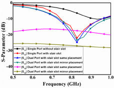
Figure 2. S-parameter variation with single- and dual-port antenna without any MS absorber.
The axial ratio fluctuation with and without a stair-shaped slot (with equal and unequal arm length) is depicted in Fig. 3. When a stair-shaped slot with uneven arm length is loaded, Fig. 3 shows that the axial ratio falls below 3 dB within the working region. The stair-shaped slot separates the E-field into two orthogonal components with roughly equal amplitude. The arm length variation produces the 90° phase shift between the orthogonal field components. It is a prerequisite for the creation of circular polarization (CP) waves [Reference Nasimuddin, Chen and Qing41].

Figure 3. Axial ratio variation with and without loading of stair-shaped slot.
Currently in development is a MS absorber unit cell that can reduce multipath reflection and imprecise RFID reading. A perfect MS absorber is one that balances external coupling and internal losses to prevent reradiation. By balancing the transmission and reflection power coefficients, this is accomplished. Since the structure’s backside is completely covered in copper, the transmission coefficient is 0, allowing the absorptivity (A) to be calculated by
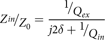
The inherent losses of resonant unit cells significantly restrict the overall achievable absorption. Effective dielectric losses with the right impedance matchings or the addition of internal losses through the use of resistive materials are two potential ways to further enhance the absorption properties. Changing the external coupling as an alternative to changing the internal losses is another way to regulate the absorption process. This statement can be understood by calculating the input impedance of MS near to resonance. It is given as follows [Reference Balanis42]:
 \begin{equation}{Z\raise0.7ex\hbox{${_{in}}$} \!\mathord{\left/
{\vphantom {{_{in}} {{Z_0}}}}\right.}
\!\lower0.7ex\hbox{${{Z_0}}$}} = \frac{{{\raise0.7ex\hbox{$1$} \!\mathord{\left/
{\vphantom {1 {{Q_{ex}}}}}\right.}
\!\lower0.7ex\hbox{${{Q_{ex}}}$}}}}{{j2\delta + {\raise0.7ex\hbox{$1$} \!\mathord{\left/
{\vphantom {1 {{Q_{in}}}}}\right.}
\!\lower0.7ex\hbox{${{Q_{in}}}$}}}}{\text{ }}\end{equation}
 where ![]() $\delta $ = (ω − ω0)/ω0 is the detuned degree, ω0 is the angular resonant frequency, Qin and Qex are the internal and external Q-factors, respectively, and Z0 is the impedance in free space. It is easily deduced from (A) that a locus of Zin forms a circle on the Smith chart with the diameter of 2Qin/(Qin + Qex), assuming that Qin and Qex are constant at the resonance. Since the impedance circle passes the origin (zero reflection) at the resonance, a complete absorption happens at the critical coupling of Qin = Qex. Whereas Qex originates from the external coupling between the guided waves in the MS and the normal incident waves, Qin originates from the conductor and dielectric losses in practical MSs [Reference Mumby and Yuan43, Reference Zhao, Zhu, Dong, Lv, Li, Guan, Shi and Zhang44]. Reflection coefficient (|S11|) in terms of internal losses (
$\delta $ = (ω − ω0)/ω0 is the detuned degree, ω0 is the angular resonant frequency, Qin and Qex are the internal and external Q-factors, respectively, and Z0 is the impedance in free space. It is easily deduced from (A) that a locus of Zin forms a circle on the Smith chart with the diameter of 2Qin/(Qin + Qex), assuming that Qin and Qex are constant at the resonance. Since the impedance circle passes the origin (zero reflection) at the resonance, a complete absorption happens at the critical coupling of Qin = Qex. Whereas Qex originates from the external coupling between the guided waves in the MS and the normal incident waves, Qin originates from the conductor and dielectric losses in practical MSs [Reference Mumby and Yuan43, Reference Zhao, Zhu, Dong, Lv, Li, Guan, Shi and Zhang44]. Reflection coefficient (|S11|) in terms of internal losses (![]() $\frac{1}{{{\tau _0}}}$) and external coupling (
$\frac{1}{{{\tau _0}}}$) and external coupling (![]() $\frac{1}{{{\tau _e}}}$) is given as follows [Reference Zhao, Zhu, Dong, Lv, Li, Guan, Shi and Zhang44]:
$\frac{1}{{{\tau _e}}}$) is given as follows [Reference Zhao, Zhu, Dong, Lv, Li, Guan, Shi and Zhang44]:
 \begin{equation}\left| {{S_{11}}} \right| = \frac{{\left( {\frac{1}{{{\tau _e}}}} \right) - \left( {\frac{1}{{{\tau _0}}}} \right)}}{{\left( {\frac{1}{{{\tau _e}}}} \right) + \left( {\frac{1}{{{\tau _0}}}} \right)}}{ }\end{equation}
 For  $\left( {\frac{1}{{{\tau _e}}}} \right) = \left( {\frac{1}{{{\tau _0}}}} \right)$, i.e. the resonant frequency, there is no reflection, meeting the critical coupling requirement. It should be mentioned that the resonator is said to be over coupled when
  $\left( {\frac{1}{{{\tau _e}}}} \right) \gt \left( {\frac{1}{{{\tau _0}}}} \right)$, and under coupled when
  $\left( {\frac{1}{{{\tau _e}}}} \right) \lt \left( {\frac{1}{{{\tau _0}}}} \right)$. The rate of power escape from the resonant structure (MS absorber at resonance) is higher in the overcoupled area than the rate of internal dissipation. When considering the undercoupled scenario, internal losses surpass power leakage from the structure in terms of quantity.
The current study aims to meet the critical coupling requirement irrespective of the unit-cell size by optimizing that method in the megahertz range. We want to show how a straightforward unit cell with good reflection properties may be tuned to be the ideal absorber for normal incident waves on a substrate of the same dimensions and kind. Perfect absorption was attained by altering the external connection, which was accomplished by appropriately slicing diagonal slits on the metal circular patch. The patch underwent a first diagonal incision to lengthen the current channel and lower the resonance frequency. It also caused the region to become undercoupled as opposed to overcoupled. To symmetrize the E distribution locally with regard to the incident wave polarization – which is concentrated along the y-axis at the unit cell edges – a second slot was incorporated into the construction. This situation is explained in detail in Fig. 4, which shows the E-field distribution in three different scenarios: (a) an unslotted patch; (b) a circular patch with a single diagonal slit; and (c) a circular patch with two diagonal slits.
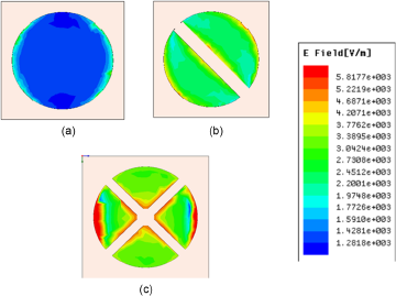
Figure 4. E-field distribution at the top surface of the unit-cell design stages for an 868 MHz normal incident plane wave (a) circular patch without any slit (b) circular patch with one diagonal slit (c) circular patch with two diagonal slits.
It is crucial to keep in mind that the Poynting theorem links the imaginary component of permeability and permittivity to the real part of the mean power as time passes. Therefore, one of the most important factors in achieving 100% absorption is the dielectric tanδ. The Poynting theorem states that the real components of the meta-surface absorber (MSA) permittivity (ε) and permeability (μ) are engaged with the resonance of the MSA along the incident wave’s path [Reference Bao, Ruvio and Ammann45, Reference Augustin, Rao and Denidni46]. This explains why the stored power in the near-field of MEH switches between reactive magnetic and electric fields with each time-harmonic field cycle. While these components are necessary to generate the MSA resonance, they may be disregarded in order to compute the actual portion of average power [Reference Bao, Ruvio and Ammann45, Reference Baggen47]. On the other hand, at the resonance frequency of MEH, the imaginary components of ε and μ operate as power consumption, and a real resistance may mimic the EM response [Reference Bao, Ruvio and Ammann45]. It should be noted that an equal quantity of magnetic and electric energy may be carried by an EM wave traveling in free space. This is because, prior to exchanging their energy with the energy of the meta-atom, these traveling waves are in a balanced condition at the free-space medium [Reference Baggen47]. In fact, this balance is maintainable, and in a perfect MS with no reflections, the majority of the incoming wave’s actual average power is used at the loads. In this instance, the latter was accomplished by managing exterior bonding on a low-loss unit-cell material that had a tanδ of just 0.0015.
To demonstrate how the loss tangent influences absorbent properties, Fig. 5 simulates the absorption variation of the suggested unit cell with change in tanδ. At unity magnitude, the behavior of the lossless unit cell is similar to that of a typical HIS reflector, and at tanδ = 0.0015, nearly total absorption was achieved. Figure 6 displays the fluctuation of the S-parameter with and without the MS absorber after the unit cell has been converted into an array and put on the bottom part of the radiator. Figure 6 presents that the properties of the reflection coefficient are about the same in both scenarios. In other words, the intrinsic characteristics of the antenna remain unaffected by the suggested MS absorber’s loading. In all scenarios, there is about the same isolation among the ports. The gain fluctuation with and without an MS absorber is exposed in Fig. 7. It can be perceived from Fig. 7 that the inclusion of an MS absorber increases the gain value to 2–3 dBi. Notably, |S11| can approach 0 over a substantial percentage of the proposed absorber, in contrast to iigh-impedance surface, where the |S11| magnitude at the resonant frequency is 1. Thus, the absorber in combination with the normal patch antenna not only yields a noticeable gain boost but may also help enhance the fading situation of RFID schemes by decreasing the severe complex replication interference and crash difficulties.

Figure 5. Absorptivity variation with change in loss tangent value.

Figure 6. S-parameter variation of dual-port antenna in presence/absence of MS absorber.

Figure 7. Gain variation of dual-port antenna in presence/absence of MS absorber.
Experimental verification and discussion
This stage involves testing the suggested antenna prototype to validate the optimum outcomes. Figure 8 shows pictures of the built prototype of the proposed antenna. It is made on FR-4 dielectric, which has a dielectric constant of 4.4. The two-port radiator is positioned beneath the MS absorber. The suggested antenna’s measured and simulated S-parameter is displayed in Fig. 9. It is tested with an E5071C vector network analyzer that is based on Keysight. It is verified by Fig. 9 that the simulated and observed S-parameters have a strong correlation. The suggested antenna has an isolation level of more than 25 dB and operates efficiently in the frequency range of 710–980 MHz.

Figure 8. Pictures of fabricated prototype of designed radiator (a) top view (b) MS absorber (b) 3D view of designed radiator.

Figure 9. Measured/simulated S-parameter of proposed antenna design.
The suggested antenna’s observed and predicted axial ratio fluctuation is displayed in Fig. 10. Dual linear pattern measuring is used to measure it [Reference Nakamura and Fukusako48]. It is evident from Fig. 10 that the simulated and observed axial ratios accord rather well. The CP waves in the range of 835–894 MHz are supported by the suggested radiator. The simulated and observed LHCP (Left handed Circular Polarization)and RHCP (Right handed Circular Polarization) far-field pattern at 0.86 GHz in the XZ plane is displayed in Fig. 11. It can be perceived from Fig. 11 shows that LHCP waves with port-1 and RHCP waves with port-2 are supported by the suggested radiator. This indicates that the polarization diversity idea is supported by the suggested antenna. The generated and measured patterns correspond rather well. The suggested antenna design’s gain change in the broadside direction is shown in Fig. 12. Two antenna approach is used to measure it [Reference Nakamura and Fukusako48]. It is verified from Fig. 12 that the working band’s maximum antenna gain is about 3.0 dBi.
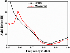
Figure 10. Measured/simulated axial ratio variation of proposed antenna.
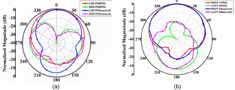
Figure 11. Measured/simulated RHCP and LHCP of proposed radiator at 0.86 GHz (a) port-1 (b) port-2.

Figure 12. Measured/simulated gain variation of proposed antenna toward broadside direction.
The diversity parameters, or the diversity gain (DG) and envelope correlation coefficient (ECC) fluctuation for the planned multiport radiator, are shown in Fig. 13. The similarity content between ports 1 and 2 is expressed by ECC. It should be low (less than 0.2) for effective radiator design [Reference Ghaneizadeh, Joodaki, Börcsök, Golmakani and Mafinezhad49]. The gain of a multiport radiator in a fading environment is expressed as DG. Its value for an efficient antenna is around 10.0 dB [Reference Ghaneizadeh, Joodaki, Börcsök, Golmakani and Mafinezhad49]. It is verified from Fig. 13 that, within the operational band, the value of DG is around 10.0 dB and the value of ECC is less than 0.1. Table 1 is used to evaluate the intended radiator’s performance with other current antennas in terms of gain, axial ratio bandwidth, and antenna size. Form Table 1, it is clearly observed that the proposed antenna design first time proposed a two-port MIMO along with CP characteristics and loaded with metamaterial absorber for UHF RFID application. The proposed antenna is compact in size as well as provides the good gain value as compared to other radiation structure.

Figure 13. Measured/simulated ECC and DG variation of proposed antenna.
Table 1. Performance assessment of proposed dual-port printed antenna with other existing antenna on the basis of absolute/axial ratio bandwidth, gain and antenna size

Conclusion
For RFID uses in the 0.868 GHz band, a two-port MS microstrip radiator with dual functionality – that is, antenna and absorbent modes – was presented. The antenna architecture consists of two coaxially fed patch antennas filled with stair-shaped slots and a MS absorber performing as a synthetic ground. It seemed interesting to incorporate a MS absorber into the antenna construction to create a reader antenna that can reduce fading replication and inappropriate RFID reading, which is important for the uses that are being considered. Within the operational band, which is 835–894 MHz, stair-shaped slot loading generates the CP waves. The slot’s mirror image improves isolation by more than 30 dB and offers polarization variety. The suggested antenna has a gain of 3.0 dBi, which is significantly larger than that of a traditional patch radiator. These results demonstrate that the proposed twin-port radiator can compete with existing RFID readers, indicating that it might be a good choice for future mobile or fixed RFID applications.
Funding statement
This research received no specific grant from any funding agency, commercial or not-for-profit sectors.
Competing interests
The authors report no conflict of interest.

Anand Vardhan Bhalla is pursuing PhD under the supervision of Prof. Agya Mishra at the Department of Electronics and Telecommunication Engineering, Jabalpur Engineering College, Jabalpur, Madhya Pradesh, India affiliated to Rajiv Gandhi Proudyogiki Vishwavidyalaya, Bhopal, Madhya Pradesh, India. He earned his M.Tech in Digital Communication from Gyan Ganga College of Technology, Jabalpur, Madhya Pradesh, India and his B.E. in Electronics and Communication Engineering from Indira Gandhi Government Engineering College Sagar, Madhya Pradesh, India, in 2012 and 2005, respectively. With over a decade of experience in academia, he has served as an Assistant Professor at Engineering Institutions across India. His research career spans more than 10 years, during which he has published over 35 research papers in journals of repute. He also holds two patents, reflecting his contributions to his field. His work has more than 500 citations. His research interests are broad and include Digital Communication, Artificial Intelligence, Machine Learning, IoT, and Signal Processing.

Agya Mishra is presently Head of Department of Artificial Intelligence and Data Science and Professor in Department of Electronics and Telecommunication Engineering, Jabalpur Engineering College, Jabalpur, Madhya Pradesh, India affiliated to Rajiv Gandhi Proudyogiki Vishwavidyalaya, Bhopal, Madhya Pradesh, India. Her qualification includes PhD and M.Tech from Maulana Azad National Institute of Technology, Bhopal, Madhya Pradesh, India and has done B.E. from Government Engineering College, Ujjain, Madhya Pradesh, India. She has more than 100 publications globally, having over 400 citations. She is an AI system designer, AI consultant, Academician, PhD guide and Journal reviewer.


