


Introduction
Driven by the continuous increase in the demand for high-speed communication, the data-rate supported by wireless systems has been growing constantly in the recent years. Moving the operation frequency of the links to the sub-mmWave and THz bands offers a solution to this demands, due to the high bandwidth available while working at this carrier frequencies, allowing high data-rate communication with relatively simple modulation schemes such asbinary phase keying (BPSK) and quadrature phase shift keying (QPSK). Additionally, the wavelength at this frequency is of the order of 1 mm, what allows higher level of integration such as on-chip antennas [Reference Akyildiz, Jornet and Han4].
Traditionally, only expensive solutions based on III–V semiconductors have been suitable for this frequency range [Reference Lopez-Diaz5, Reference Antes6]. Nevertheless, the recent advancement in the semiconductor process technology [Reference Lachner7] has made silicon a low-cost alternative for high data-rate communication systems above 200 GHz. Several receivers with different architectures have already been published working in the frequency band between 100 and 300 GHz based on a silicon technology [Reference Sarmah1, Reference Thyagarajan, Kang and Niknejad8–Reference Eissa11].
In [Reference Thyagarajan, Kang and Niknejad8], a QPSK receiver working at 240 GHz in a complementary metal-oxide semiconductor (CMOS) technology is presented. It has a conversion gain (CG) of 25 dB and a NF of 15 dB. Nevertheless, due to the tripler after the mixing stage, the spectral efficiency is reduced to one-third in comparison with a direct-conversion architecture, achieving a maximum speed of 16 Gbps. A CMOS receiver with a CG of − 19.5 dB, a noise figure (NF) of 27 dB and 26.5 GHz BW working at 300 GHz is presented in [Reference Hara9]. It achieves a maximum speed of 32 Gbps with a 16-quadrature amplitude modulation (QAM) in the cm distance range. A direct conversion receiver in a SiGe heterojunction bipolar transistor (HBT) technology working at 190 GHz and a 3-dB BW of 26 GHz is presented in [Reference Fritsche10]. With a CG of 47 dB and a NF of 10.7 dB it achieves a maximum speed of 50 Gbps for a link distance of 0.19 cm. A double-balanced mixer-first architecture has been realized in [Reference Eissa11]. It has been implemented in a 130 nm SiGe technology and has a RF BW of 55 GHz, a CG of 13 dB, and a NF of 18 dB. In this paper, we present a fully-integrated direct-conversion fundamentally-operated mixer-first quadrature receiver module. The chip includes an on-chip broadband ring antenna and has been fully packaged. All the measurements have been taken in a free-space setup. The high-speed IF interfaces are available at on-board connector level. The 3-dB radio frequency/local oscillator (RF/LO) BW is 47 GHz, with a peak CG of 7.8 dB and a minimum single-sideband(SSB) NF of 11.7 dB. Together with the transmitter presented in [Reference Sarmah1–Reference Rodriguez Vazquez3], the maximum speed achieved is 60 Gbps over 1 m distance.
This paper is organized as follows. The receiver top-level architecture is described inthe section “Receiver architecture”. In the section “Circuit design and simulated results”, the circuit design considerations are discussed and simulation results are presented. In the section “RF measured results”, the RF measurement setup is described and the results presented. The wireless communication link setup and results are presented in the section “Wireless link test”. A short conclusion is given in the last section.
Receiver architecture
The proposed architecture for the down-conversion mixer-first in-phase and quadrature (IQ) receiver is presented in Fig. 1. In comparison with the traditional architectures, the low noise amplifier (LNA) has been removed. At this frequency band, the LNA does not provide a NF good enough to justify the limitation in RF BW that the circuit introduces [Reference Sharma12–Reference Mao14]. The RF signal is fed directly to the mixer by a wideband lens-integrated wire-ring on-chip antenna [Reference Sharma12], which illuminates a 9-mm diameter silicon-lens placed on the Si chip rear side. The quadrature mixer consists of two double-balanced switching-quads that down-convert the RF signal. For this architecture, the mixer has to keep the NF low and the CG high to isolate the noise contribution from the following components. The down-converted IF signal interfaces a high-speed PCB through a differential baseband amplifier that acts as a buffer, providing a broadband 50 Ω output match. The quadrature of the LO is provided by a wideband differential hybrid [Reference Grzyb15]. This LO signal is generated on-chip by a broadband x16 multiplier chain, topologically similar to the one reported in [Reference Sarmah, Heinemann and Pfeiffer16]. It is realized by cascading four broadband Gilbert-cell doublers. The LO input-drive in the 13.6–16.7 GHz frequency range is provided in a single-ended mode at the board connector level and converted to differential-mode on-chip by an active balun. The x16 multiplication factor was chosen as a compromise between on-chip complexity level and board-level performance. The multiplier chain is followed by a 3-stage differential-cascode power amplifier, which delivers enough LO power to operate the quadrature mixer for maximum CG and minimum NF.
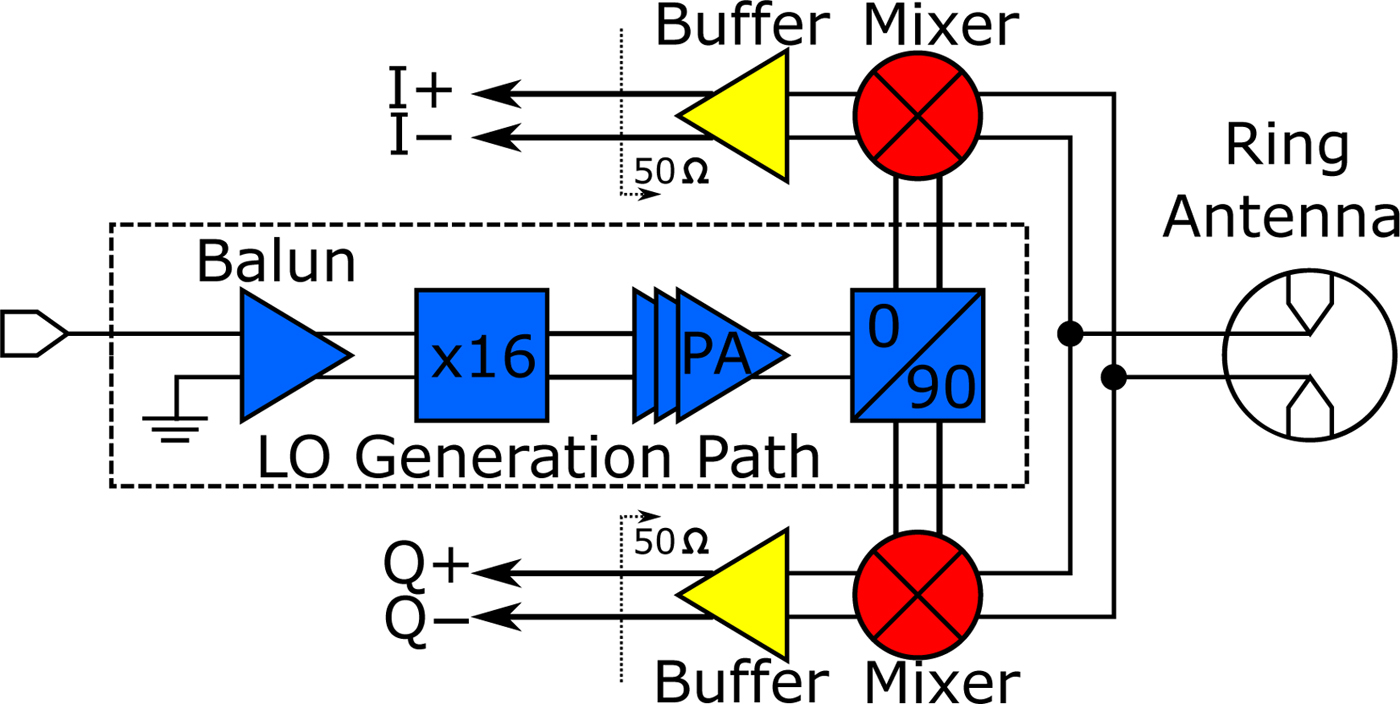
Fig. 1. Block diagram of the IQ direct-conversion mixer-first receiver.
Circuit design and simulated results
The receiver was fabricated in an experimental 0.13 μm SiGe HBT technology in the frame of the DOTSEVEN project [Reference Lachner7]. This process was derived from IHP's (innovations for high performance) 0.13 μm BiCMOS technology SG13G2 [Reference Ruecker17] where the annealing was optimized and the minimum emitter dimension was reduced from 120 nm to about 100 nm, leading to enhanced peak fT/fmax of 350/550 GHz.
Figure 2 shows the double-balanced fundamentally-operated down-conversion mixer with the baseband amplifier used at the outputs of both IQ channels. In comparisonwith the standard Gilbert-cell mixer topology [Reference Sarmah1], the transconductance stage has been removed, eliminating the capacitive internal node between this stage and the switching-quad. This leads into an improvement in the RF operating bandwidth of the receiver. The noise contribution of this stage has also been removed. In order to operate the mixer with the maximum CG and minimum NF, the switching-quad has to be biased around the onset of active forward operation and the LO drive has to be high enough at the base nodes to minimize the time when both quads differential pairs are on during the LO transition events. On the other hand, the realization of the receiver CG has to be moved to the baseband. A dc-coupled differential amplifier has been added to increase the receiver gain and to match the output impedance to 50 Ω.
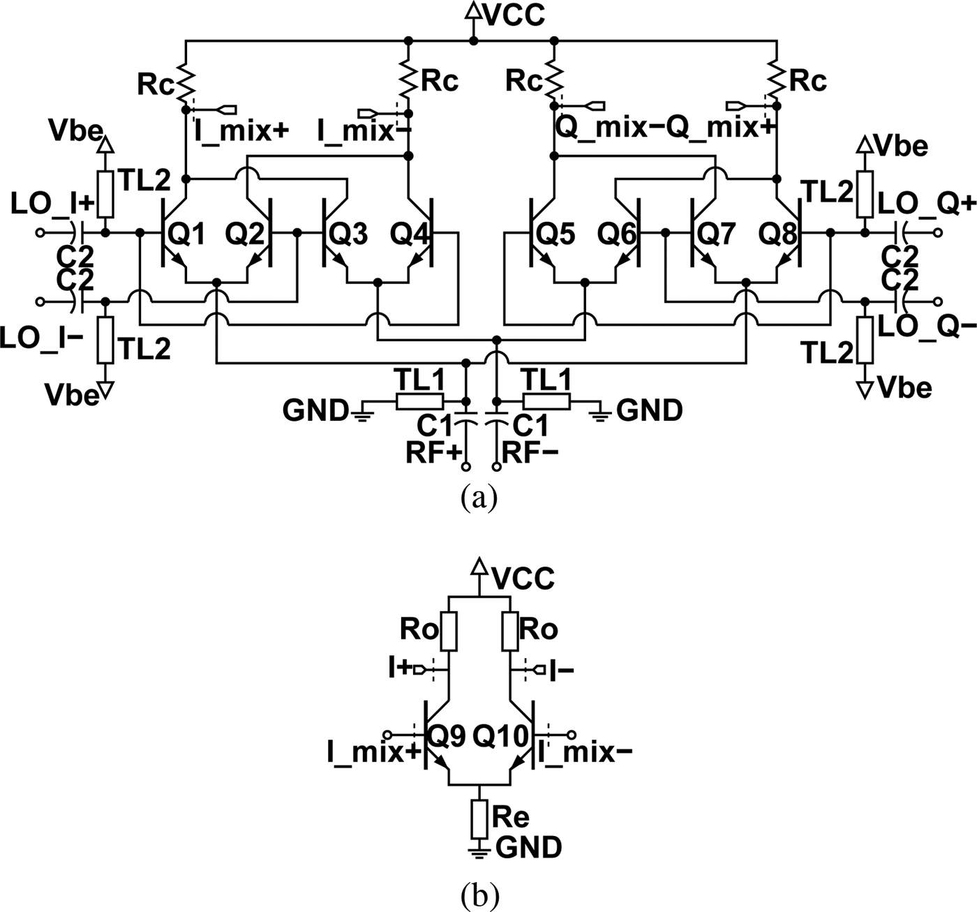
Fig. 2. Schematic of the quadrature direct-conversion mixer (a) and one of the output IF buffer (b).
The emitter area has been chosen to be twice the minimum size for the transistors in the mixer. The emitter-fed RF input presents an impedance profile constant for the operational frequency. Hence, the RF matching network has been co-designed with the antenna to provide a broadband match at the RF port for differential signals. It consists of a shorted 50 Ω TL1 stub of 45 μm, used also as a dc-current path, and a series metal-isolator-metal (MIM)-capacitor C1 = 52 fF. The LO matching network includes a 50 Ω transmission line TL2 of 80 μm, used for base biasing as well, and a series MIM-capacitor C2 = 60 fF. The resistors Rc at the collectors are used as IF output loads. They have a value of 260 Ω, chosen as a compromise between CG and bandwidth. The mixer output has been connected (dc-coupled) to the baseband amplifier input. This node sets a trade off between the CG, NF, and IF bandwidth. The resistor Re = 160 Ω shifts the dc-level at the emitter of the differential pair for proper biasing. The load resistors Ro = 50 Ω at the collectors set the output impedance to 50 Ω.
In order to set the operation point of the chip properly, contour plots of the CG and the NF against the mixer VBE and the LO power at the input of the hybrid have been analyzed (Fig. 3) at 240 GHz. This simulation includes the hybrid, the mixer, and the baseband amplifier. The high current models (HICUM) transistor model has been used for all the simulations. For optimum performance in both parameters, the LO power needs to be maximized in order to provide hard-switching conditions in the quad. The mixer VBE ranges between 0.58 and 0.65 V, providing a low-static bias current to minimize the NF. The mixer alone has a simulated RF/IF 3-dB bandwidth that exceeds 70 GHz with a CG of 0 dB and a NF of 11 dB. The mixer together with the baseband amplifier has a simulated 3-dB RF/IF bandwidth of 36 GHz. The simulated 1-mm long wire-bond interconnects limit the on-board 3-dB IF bandwidth to 14 GHz. Therefore, no more bandwidth on-chip is required. The simulated peak CG for the entire chip is 8 dB and the minimum NF 13 dB. The mixer consumes a current of 10.5 mA and the buffer 15.4 mA from a 2.5 V and 3.2 V power supply, respectively.
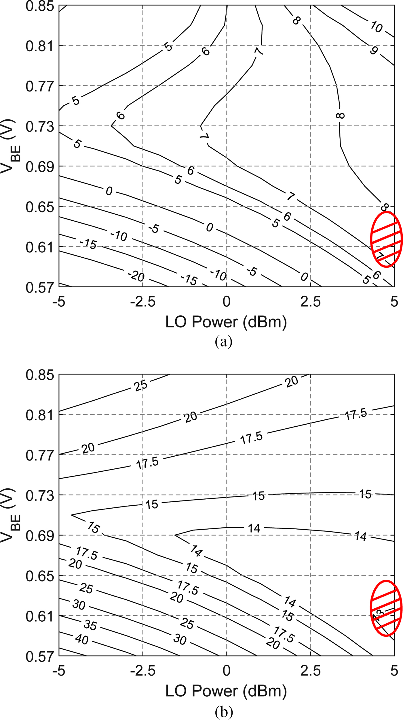
Fig. 3. Contour plot of the CG (a) and NF (b) for both IQ channels combined versus LO power at the input of the hybrid and the mixer VBE. The operating region is marked in red.
The LO generation path is topologically similar to the one presented in [Reference Sharma12]. Therefore, a detailed discussion of the circuit design has been skipped in this paper. The one used in this receiver presents improvements in the technology and redesigns in the matching networks. The multiplier chain consists of four cascaded Gilbert-cell doublers. A three-stage power amplifier (PA) is used to generate enough power to drive the the mixer. To provide the correct drive to the quadrature mixer, the LO power is split by a broadband differential coupled-line coupler (110 μm long) [Reference Grzyb15] exploiting a combination of both broadside and edge coupling between four strips located ontwo different buried metal layers for maximum operation bandwidth for the tunable LO path. The simulated LO power at the output of the PA and at both outputs of the hybrid, its amplitude-imbalance and phase-imbalance are presented in Fig. 4. The power amplifier delivers a maximum simulated power of 4.1 dBm at the input of the hybrid and its 3-dB bandwidth is 60 GHz. The simulated amplitude-imbalance between the in-phase and quadrature outputs of the hybrid is better than 0.6 dB and the phase-imbalance is below 2.5° for the 200–300 GHz band. The hybrid insertion loss is better than 0.6 dB for the 200–300 GHz band. The entire LO generation path draws a current of 135 mA from a 2.8 V power supply. For a supply voltage of 4 V the LO power at the PA output reaches 9 dBm. However, this does not result into a CG or NF improvement in the receiver, but only to an increase in the power consumption. The chip micrograph with the on-chip antenna is shown in Fig. 5. The main limitation for the IF operation bandwidth is the parasitic inductance of the 1-mm wire-bond interconnection. In order to maximize the available IF bandwidth, an on-board 8-section Butterworth-based step-impedance microstrip-line low-pass filter has been implemented on a low-cost high-speed 0.338 mm thick Rogers 4350B PCB. No additional compensation structures were applied on the chip-level. The filter was optimized using 3-D full-wave electromagnetic (EM) simulations to provide minimum group delay variations. These results were combined with the rest of the receiver for a full system simulation. The results are shown in Fig. 6. The simulated RF/IF channel 3-dB bandwidth is 28 GHz, independently of the chosen LO frequency. The conversion gain ranges between 6 and 8 dB and the amplitude imbalance stays under 0.7 dB. The simulated NF has a constant value of 13 dB for the entire operational BW. The simulated group delay between the mixer input and the filter output presents a variation of ±10 ps in the operating band. This value is dominated by the on-board filter, whose electrical length is orders of magnitude bigger than the on-chip circuits. This introduces also the ripples that can be observed in the CG and group delay plots.
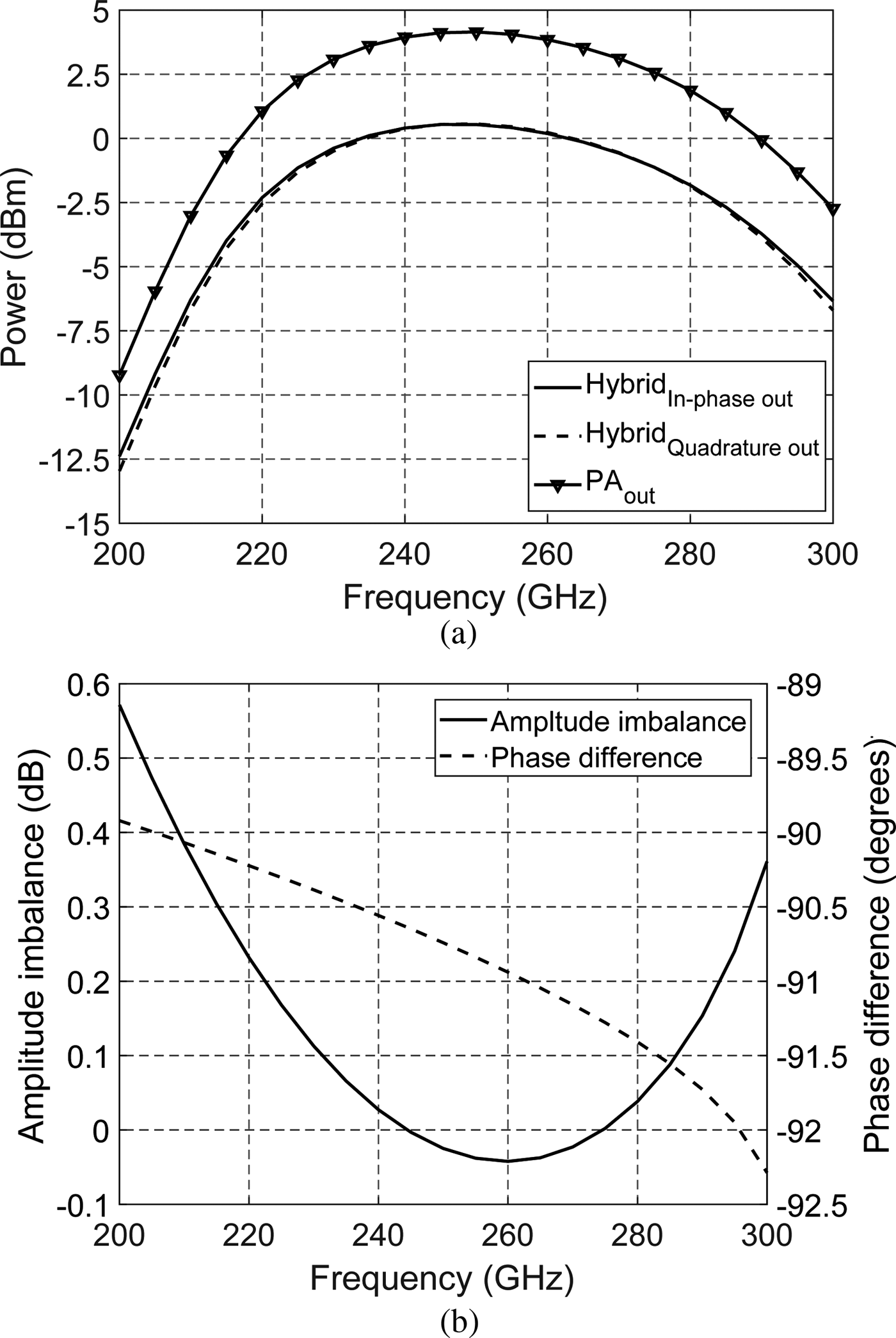
Fig. 4. Simulated power at the output of the PA and the hybrid (a) and amplitude-imbalance and phase difference (b) at the output of the hybrid.
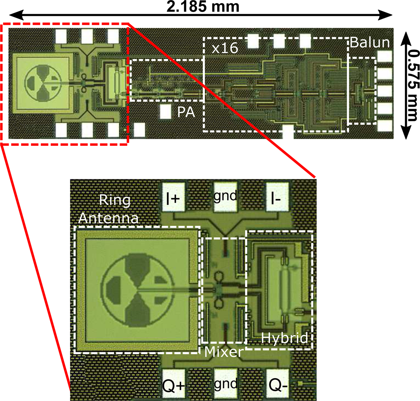
Fig. 5. Chip micrograph of the receiver.
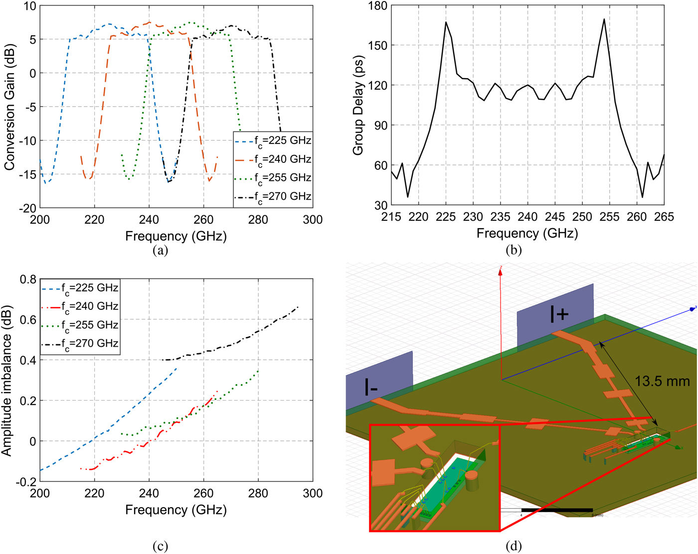
Fig. 6. Simulated receiver RF/IF BW for IQ channels combined at different carrier frequencies (a), group delay (b), IQ amplitude imbalance, (c) and 3-D model of the IF filter. (d) The 3-dB BW is 28 GHz, independently of the carrier frequency, with in-band ripples under 1 dB. The group delay is only plotted for a carrier frequency of 240 GHz. It is similar at other carrier frequencies, with variations under 1% for different carriers. The amplitude imbalance stays below 0.7 dB.
The receiver chip is glued on the back side of a high resistivity hyper-hemispherical silicon 9-mm diameter lens with the on-chip ring antenna aligned with the lens center. For the complete antenna-lens assembly in combination with a 9-mm hyper-hemispherical lens with an elliptical extension, the EM-simulations predict an input reflection better than − 19 dB and antenna directivity of 23.3–26.3 dB for 205–285 GHz. For the on-chip antenna radiating into a hypothetical lossless silicon half-space through a 150 μm thick lossy chip, the simulated radiation efficiency is higher than 80%. Additionally, antenna implementation loss in the receive operation mode is incurred by the reflections at the lens--air interface. The chip-on-lens assembly is mounted on the high-speed PCB, which has a recess to accommodate the chip. A copper heat sink with a direct thermal contact to the silicon lens has been added to improve heat dissipation (Fig 7(a)).
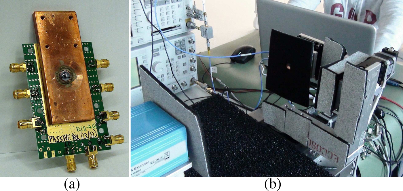
Fig. 7. Receiver module (a) and picture of the measurement setup (b) The chip is fixed to the lens with epoxy and assembled on a broadband PCB. The set up is completely covered by absorbers to reduce the impact of reflections.
RF measured results
A free-space setup was used to characterize the receiver module (Figs 7 and 8). All measurements were done at board connector level and also included the losses of the antenna. A WR-03 (220–325 GHz) frequency extension module from OML, equipped with a linearly polarized horn antenna with a directivity of 20 dBi at 270 GHz, operating in the transmit mode was used to characterize the receiver. Its output power was previously calibrated with a PM4 calorimeter. The Rx was mounted on a precision alignment 2-D rotational stage controlled by a stepper-motor. The measurements were done in the far-filed zone.
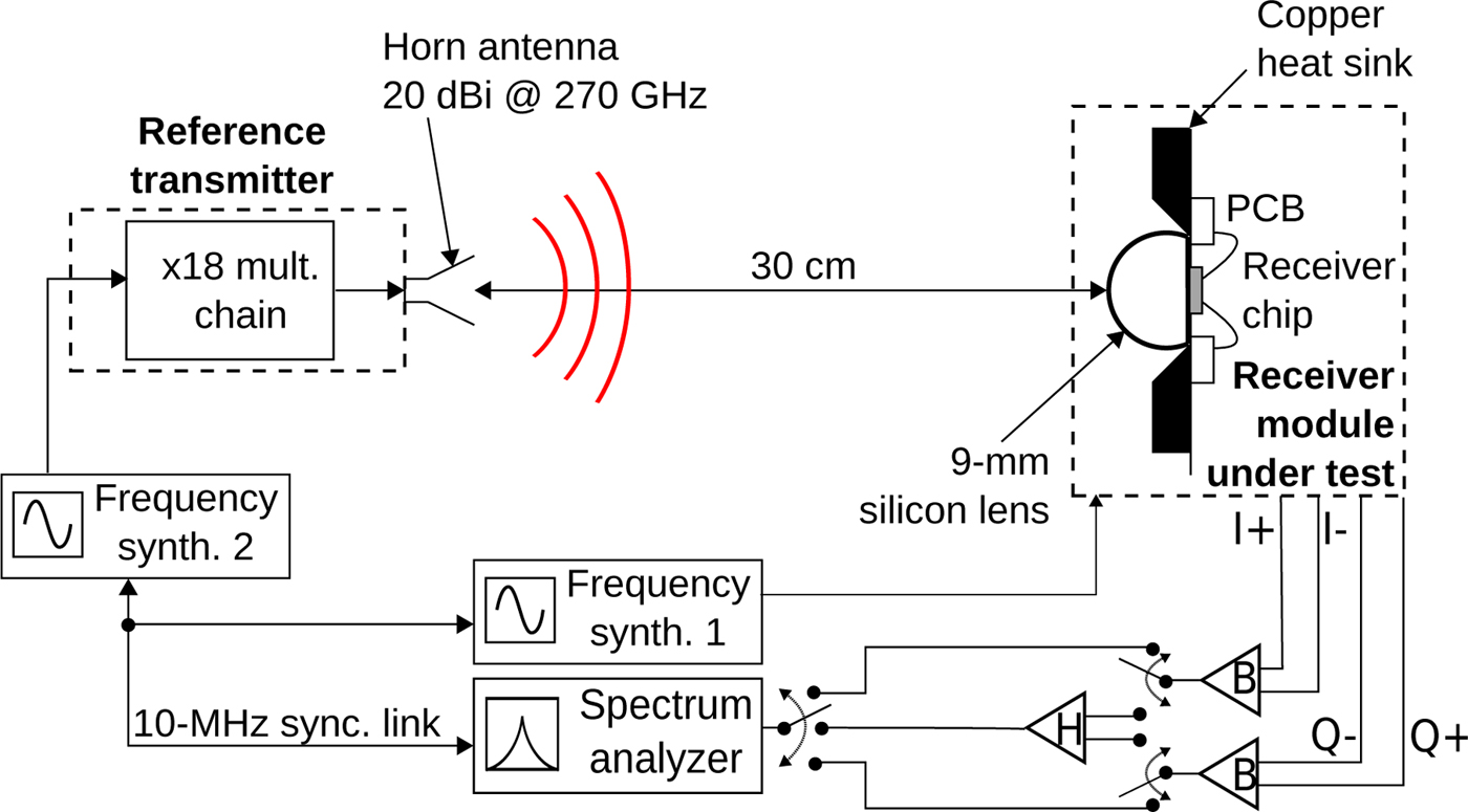
Fig. 8. Free-space characterization setup of the receiver. The differential output signals were combined with baluns (B) and a hybrid (H) was used for the SSB NF measurement.
The directivity was calculated by integrating the power density values acquired within a hemisphere sector of ±40° × ±40°. The back-side radiation was neglected, increasing artificially the directivity, because of the setup limitations. The measurement directivity varies between 25.2 dBi at 210 GHz and 27.04 dBi at 280 GHz with 26.48 dBi at 240 GHz, correlating well with the simulated results. The radiation pattern of the receiver at 240 GHz and the directivity frequency dependence are illustrated in Fig. 9.
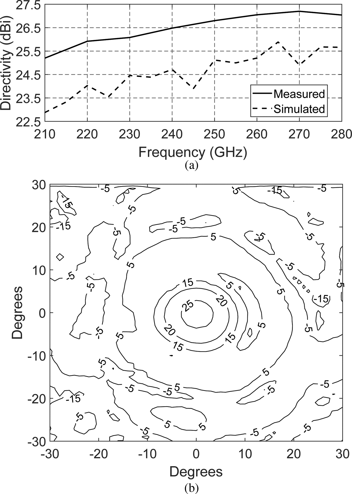
Fig. 9. Antenna directivity for the frequency band (a) and measured azimuthal view of the radiation pattern at 240 GHz (b).
For the conversion gain and IQ imbalance measurements, the receiver was aligned to the maximum directivity position. The Friis-Formula was used to calculate the power at the input of the receiver module. The measured directivity was a parameter for this calculation. The RF/LO bandwidth was first measured for a fixed IF frequency of 33 MHz between 210 and 280 GHz. The differential IQ outputs were combined using external baluns. Both IQ channels were measured separately to characterize the amplitude imbalance. Due to the lack of a noise source in our laboratory in this frequency range, the SSB NF of the receiver has been calculated from the measured conversion gain (CG) and output noise floor (Nout). The input noise floor was assumed to be N in = −174 dBm/Hz, which is the thermal noise at room temperature [Reference Ojefors18]. Figure 10 shows the results of this measurements. The maximum IQ imbalance is 1.58 dB, the peak CG is 7.8 dB, the 3-dB RF/LO bandwidth is 47 GHz, and the peak SSB NF is 11.3 dB. The ripples in the measurements are introduced by calibration errors. The measurements show a better performance than the simulations. Note that this is an experimental technology, not commercially available, and the device gain at this frequency was underestimated in the models.
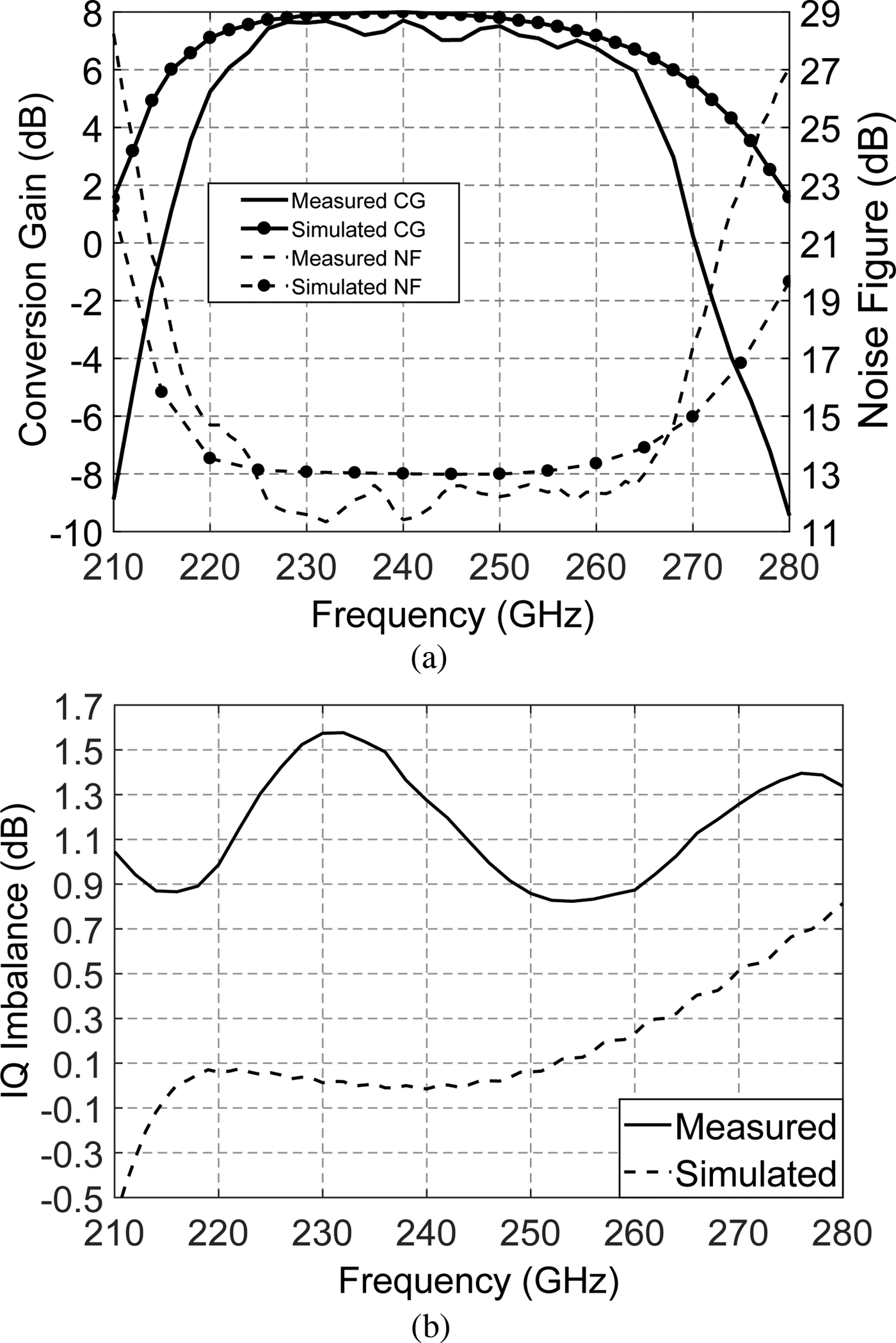
Fig. 10. Receiver CG, NF (a) and IQ imbalance (b) This measurement was performed for a fixed IF of 33 MHz.
To measure the RF/IF bandwidth of the receiver, the LO frequency was fixed to different values across the RF band (225, 240, and 255 GHz) and the RF frequency was swept ± 20 GHz around each of this LO frequency points. Due to the limited operational bandwidth of the baluns and the hybrid couplers, the IF outputs (I + , I − , Q + , Q − ) were measured separately. Therefore, the frequency characteristics for the different outputs might present minor variations depending on the differences in the assembly process and the imbalance. The loss of the connecting cables was de-embedded and only the loss of the on-board interconnects as well as the connectors is included in the presented values. The measured RF/IF bandwidth is 26 GHz. The RF/IF NF was calculated by measuring the receiver output noise at a single IF connector using the same method described before. For this measurements, the noise contribution from the different IF outputs was supposed to be uncorrelated. This uncorrelation was verified for an IF frequency of 33 MHz. Due to this, the theoretical RF/IF SSB NF is 6 dB better than the value plotted in Fig. 11 (3 dB from the differentially driven output signal and another 3 dB from the quadrature signal). Due to the IQ imbalance, the real improvement in the SSB NF will be always below this estimation.
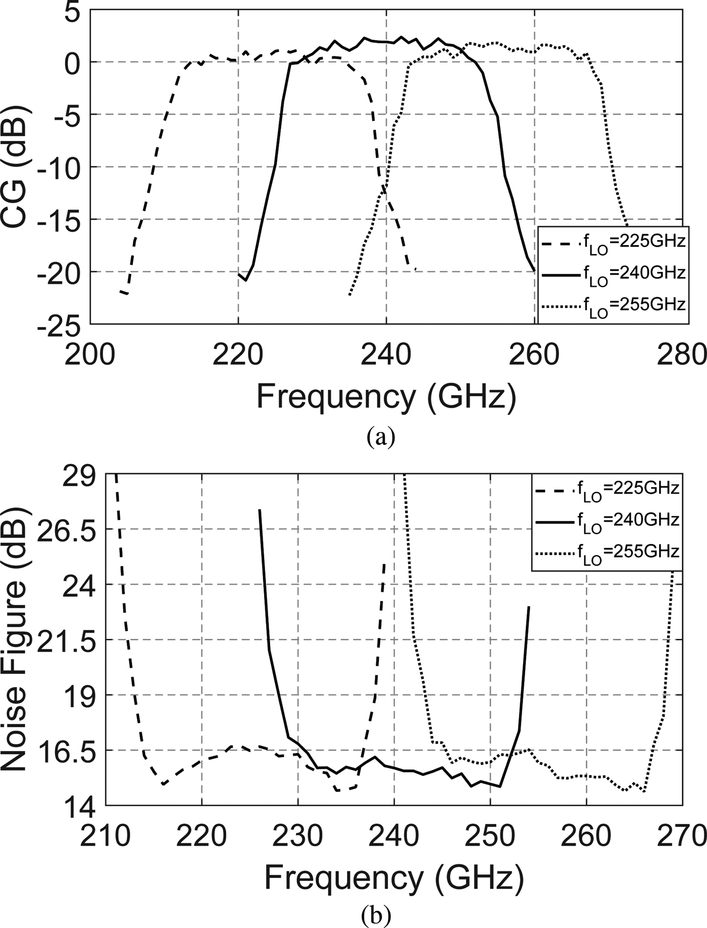
Fig. 11. Measured channel bandwidth (a) and NF (b) of the receiver for different carrier frequencies.
The LO-to-RF power leakage available at the receiver antenna was calculated as difference between the leaking power and the simulated LO power drive at the hybrid input. For this, the OML module was configured into the receive mode and its CG calibrated with a second OML module. The measured leakage was below − 30 dBm for the operational 210–280 GHz band, showing an isolation better than 35 dB.
For the linearity measurements, a VDI AMC-378 high-power source equipped with a tripler at the output capable of delivering up to 5 mW at 240 GHz was used instead of the OML module. A power calibration was performed with the PM4 calorimeter prior to the measurements. The results of this measurement are presented in Fig. 12. While operating in the antenna far-field zone, the maximum power delivered at the receiver antenna was −14.5 dBm, hence, it did not compress. Measurements for a shorter distances were performed and compression in the CG was observed. Nevertheless, this distance did not ensure far-field measurements, which changes the antenna directivity and might corrupt the results.
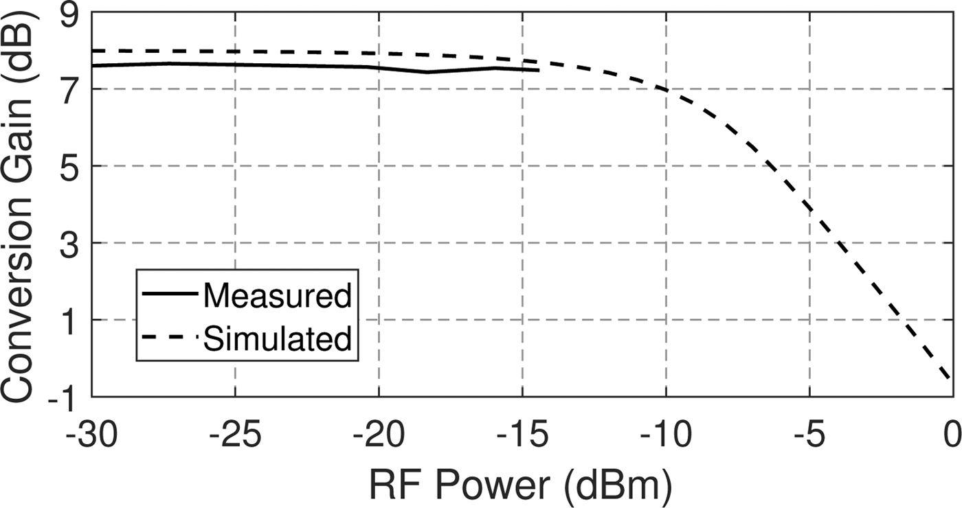
Fig. 12. Linearity of the receiver. The simulated P 1 dB is − 10 dBm at 240 GHz. Due to the free-space setup, the maximum power available at the input of the receiver is − 14.5 dBm. Therefore, the P 1 dB was not reached in the measurements.
Wireless link test
For the high-speed communication test, the transmitter presented in [Reference Sarmah1–Reference Rodriguez Vazquez3] was used. It has a compression output power of 8.5 dBm and a RF/LO bandwidth of 35 GHz measured in free-space. The Tx and Rx were synchronized and the distance was set to 1-m. To feed the differential in-phase and quadrature inputs of the transmitter, two Tektronix AWG70000 arbitrary waveform generators were used, with 18 GHz analogue-bandwidth each. As data source, a pseudo random bit sequence of order 9 was digitally modulated using BPSK. To reduce the spectral spread of the signal and to fit into the measured 13 GHz RF/IF 3-dB bandwidth of the receiver, a root raised cosine filter (α = 0.7) was applied to the modulated data stream. To measure the received signals, the differential IF outputs of the receiver were connected to two differentially driven DPO70000SX real time oscilloscopes, an analogue-bandwidth of 33 GHz each. The noise floor of the scopes is higher than for the receiver, introducing a limitation in the final signal to noise ratio (SNR). For this reason, the signal was pre-amplified using four PSPL588L broadband amplifiers. The signal quality was analyzed using SignalVu vector signal analysis software. This software facilitates clock recovery, IQ imbalance correction and adaptive channel equalization and also analyses the EVM, constellation, and eye diagram in real time. To find the bandwidth of the modulated signal at the arbitrary waveform generator (AWG) output, the AWG and the scope were connected back-to-back to measure the 90% power-contained bandwidth of the signal. The EVM provided directly from the AWG was also measured. The results of this measurement are presented in Table 1.
Table 1. Data rates versus effective BW measured back to back
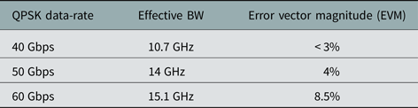
At 60 Gbps the effective BW was expected to be bigger than 16 GHz. However, the measurement shows that the AWG does not deliver this bandwidth. This introduces a limitation from our setup that leads into a higher EVM at this speed for the communication test. Nevertheless, the measured channel effective bandwidth of the 50 Gbps signal fits good the measured RF/IF bandwidth of the receiver. Measurements for different speed and carrier frequencies were performed. The constellation and eye diagrams for 50 Gbps are shown in Fig. 13. It presents an EVM of 19%. The maximum speed measured was 60 Gbps with an EMV of 26.2%. According to the tables presented in [Reference Shafik, Rahman and Islam19] for EVM and bit error rate (BER) comparison, for QPSK at 60 Gbps the estimated BER stays below 10−3 and for 50 Gbps and below it descend to a value under 10−6.
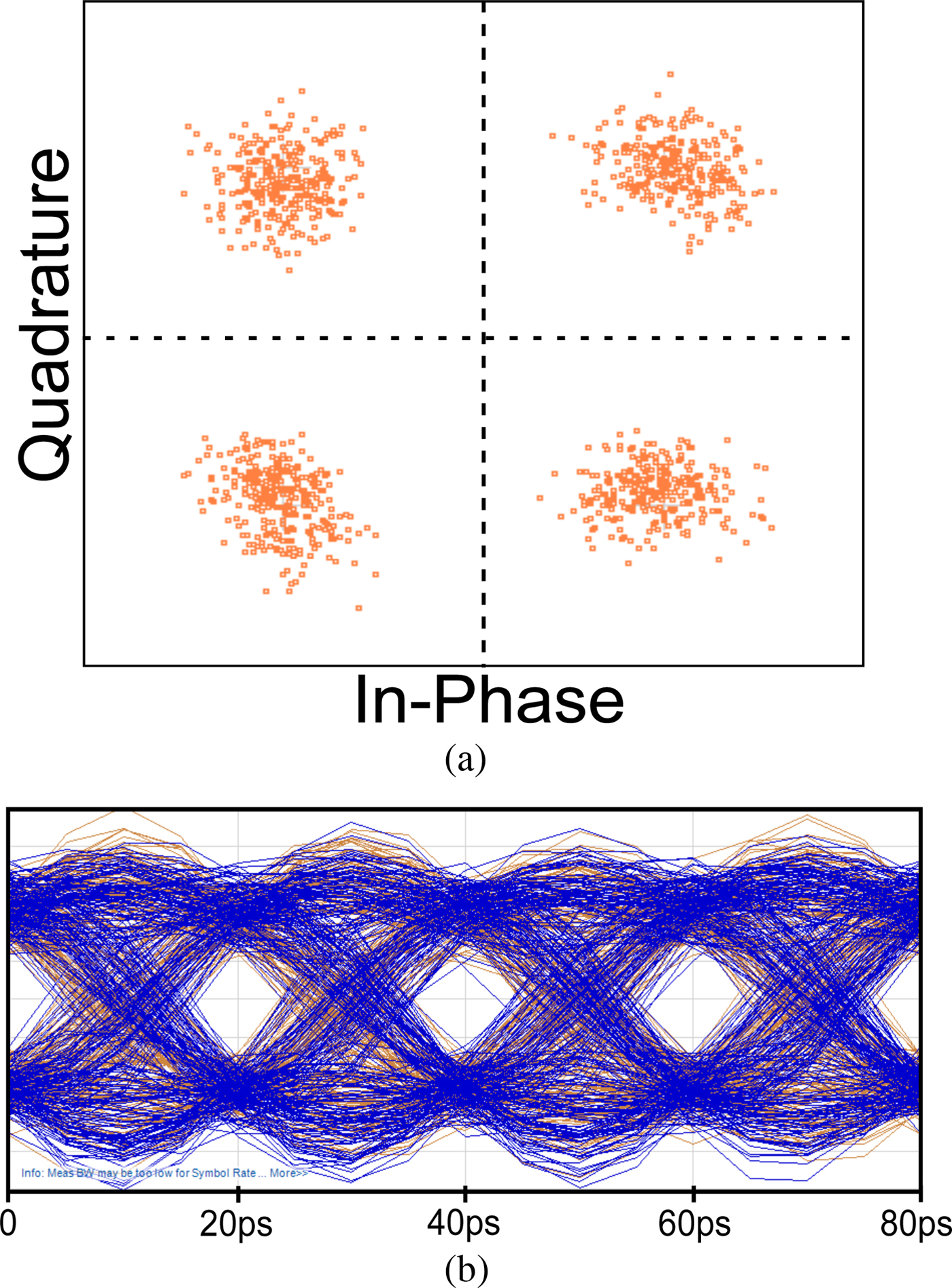
Fig. 13. Constellation (a) and eye diagram (b) for 50 Gbps QPSK working at a carrier frequency of 240 GHz (EVM=19%).
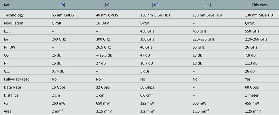
Table 2. Performance summary and comparison
Conclusion
In this paper, a fully-integrated direct-conversion mixer-first quadrature receiver module is presented. By removing the LNA between the mixer and the antenna, the RF bandwidth is enhanced with no degradation in the NF of the system. It achieved a LO tunability of 47 GHz, a 3-dB RF/IF bandwidth of 26 GHz, a CG of 8 dB and a SSB NF of 11.3 dB. The simulated group delay including the high-speed packaging presents a variation of ±10 ps for the operating bandwidth. It dissipates 455 mW, including the LO chain, and occupies 1.25 mm2. Together with the transmitter presented in [Reference Sarmah1–Reference Rodriguez Vazquez3], it achieves a maximum data-rate of 60 Gbps in a link of 1-m.
Acknowledgments
This work was partially funded by the German Research Agency (DFG) within the project Real100G.RF. and by the European Comission within the project DOTSEVEN.
 Pedro Rodriguez Vazquez received the M.Sc degree in telecommunication engineering from the University of Málaga, Málaga, Spain, in 2013. Since 2014, he is with the Institute for High-Frequency and Communication Technology (IHCT), University of Wuppertal, Wuppertal, Germany, as a Research Assistant. His research interest is in the area of material characterization and wireless communications circuits and systems at sub-millimeter-wave frequencies.
 Janusz Grzyb received the M.Sc. degree (cum laude) in electronic engineering (with a major in the synthesis and design of analogue CMOS and BiCMOS circuits with an individual study program) from the Integrated Circuits Laboratory, Technical University of Gdansk, Gdansk, Poland, in 1998, and the Ph.D. degree from the Swiss Federal Institute of Technology, Zurich, Switzerland, in 2004. From 1998 to 1999, he was a Research Assistant. In 1999, he joined the Electronics Laboratories, Swiss Federal Institute of technology, where he performed pioneering work in the area of low-cost large-area panel-processing MCM-based SiP solutions for 60-, 77-, and 94-GHz applications. From 2004 to 2006, he was with the Communication System Design and High-Speed/Optical Packaging Groups, IBM T. J. Watson Research Center, Yorktown Heights, NY, USA, where he developed package-integrated antenna and packaging solutions for millimeter-wave communication systems. From 2006 to 2009, he was with the Research and Development Group, Huber & Suhner, Pfaeffikon, Switzerland, where he brought onto the market one of the world first commercially available point-to-point 60-GHz links: the Sensity Link System. Dr. Grzyb was a co-recipient of the 2006 Lewis Winner Award for Outstanding Paper of the IEEE International Solid-State Circuit Conference, the 2006 IBM Pat Goldberg Memorial Best Paper Award, and the 2012 Jan Van Vessem Award for the Outstanding European Paper of the IEEE International Solid-State Circuit Conference.
 Neelanjan Sarmah received the Bachelors of Technology degree in electronics and telecommunication engineering from the National Institute of Technology, Silchar, India, in 2003, the M.Sc. degree in electrical engineering (with a specialization in microelectronics) from the Delft University of Technology, Delft, The Netherlands, in 2008. and the Ph.D. degree from the University of Wuppertal, Germany, in 2016. From 2008 to 2010, he was a Research Staff Member with the German federal research institute IHP Microelectronics, where he was involved in the design of transmitter components such as frequency multipliers and power amplifiers at 120 GHz in in-house SiGe:BiCMOS technology. Since 2011, he has been a Research Staff Member of the Institute for High-Frequency and Communication Technology (IHCT), University of Wuppertal, Wuppertal, Germany. He was part of the Research Training Group GRK 1564 Imaging New Modalities. His research interests are in the area of sub-millimeter-wave circuit components and systems for high data-rate communication and material characterization in low-cost silicon technologies.
 Bernd Heinemann received the Diploma degree in physics from the Humboldt Universität zu Berlin, Berlin, Germany, in 1984, and the Ph.D. degree in electrical engineering from the Technische Universitaet Berlin, Berlin, Germany, in 1997. In 1984, he joined the IHP (now called Innovations for High Performance Microelectronics), Frankfurt (Oder), Germany. His research activities include the development and characterization of MOS and bipolar devices. From 1984 to 1992, he contributed to the development of an epi-free 0.8- m BiCMOS technology. Since 1993, he has been a member of a team involved with the exploration and technological implementation of SiGe HBTs.
 Ullrich R. Pfeiffer received the Diploma and Ph.D. degrees in physics from the University of Heidelberg, Heidelberg, Germany, in 1996 and 1999, respectively. In 1997, he was a Research Fellow with the Rutherford Appleton Laboratory, Oxfordshire, UK. In 2000, his research was based on real-time electronics for a particle physics experiment with the European Organization for Nuclear Research (CERN), Geneva, Switzerland. From 2001 to 2006, he was with the IBM T. J. Watson Research Center, where his research involved RF circuit design, power-amplifier design at 60 and 77 GHz, and high-frequency modeling and packaging for millimeter-wave communication systems. In 2007, he led the Terahertz Electronics Group, Institute of High-Frequency and Quantum Electronics, University of Siegen, Siegen, Germany. Since 2008, he has held the High-Frequency and Communication Technology Chair with the University of Wuppertal, Wuppertal, Germany. Dr. Pfeiffer is a member of the German Physical Society (DPG). He was the recipient of a European Young Investigator Award in 2007. He was a corecipient of the 2004 and 2006 Lewis Winner Award for Outstanding Paper of the IEEE International Solid-State Circuit Conference, the 2006 IBM Pat Goldberg Memorial Best Paper Award, the 2008 EuMIC Best Paper Award, the 2009 Best RFIC Oral Paper Presentation, the 2010 EuMC Microwave Prize, and the 2012 Jan Van Vessem Award for Outstanding European Paper of the 2012 IEEE International Solid-State Circuit Conference.


