Skip to main content Accessibility help
×
Hostname: page-component-745bb68f8f-grxwn Total loading time: 0 Render date: 2025-01-18T16:10:32.337Z Has data issue: false hasContentIssue false

5 - Active RF and Microwave Semiconductor Devices

Published online by Cambridge University Press:  10 November 2017

Giovanni Ghione
Affiliation:
Politecnico di Torino
Marco Pirola
Affiliation:
Politecnico di Torino
Get access

Summary

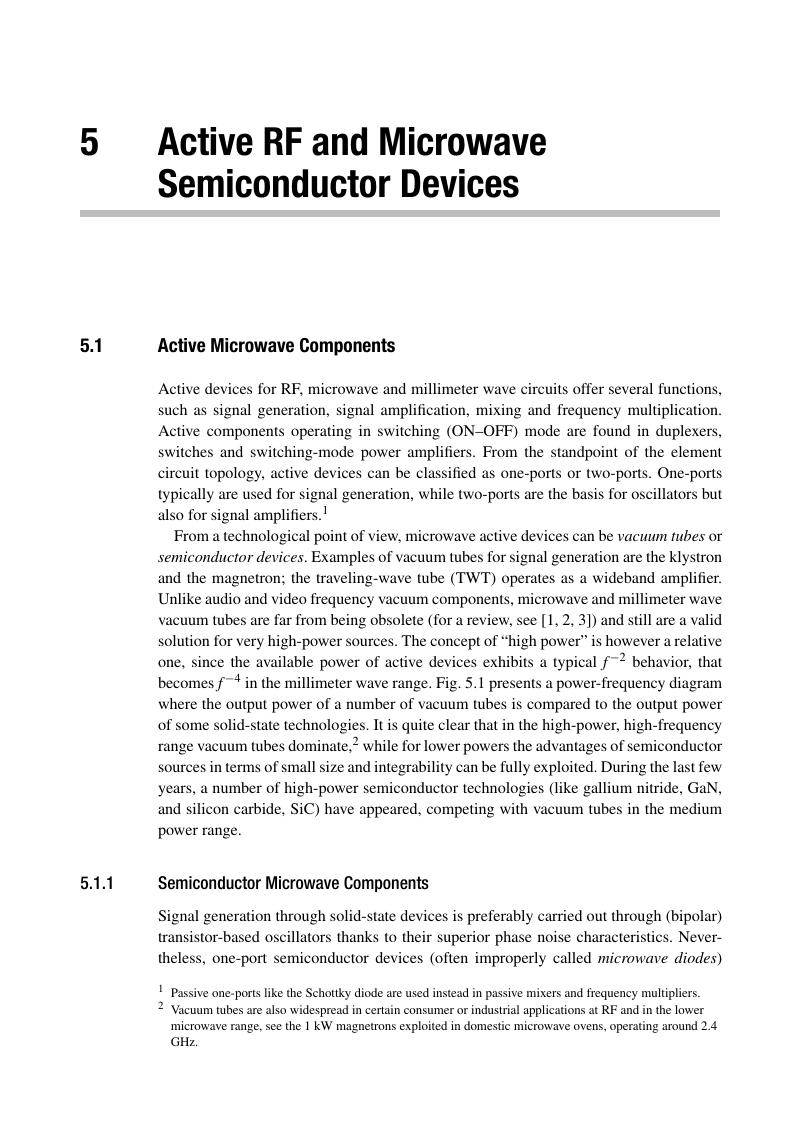
Image of the first page of this content. For PDF version, please use the ‘Save PDF’ preceeding this image.'
Type
Chapter
Information
Microwave Electronics , pp. 185 - 260
Publisher: Cambridge University Press
Print publication year: 2017

Access options

Get access to the full version of this content by using one of the access options below. (Log in options will check for institutional or personal access. Content may require purchase if you do not have access.)

References

[1] J. X., Qiu, B., Levush, J., Pasour, A., Katz, C. M., Armstrong, D. R., Whaley, J., Tucek, K., Kreischer, and D., Gallagher, “Vacuum tube amplifiers,IEEE Microwave Magazine, vol. 10, no. 7, pp. 38–51, Dec. 2009.Google Scholar
[2] J. H., Booske, R. J., Dobbs, C. D., Joye, C. L., Kory, G. R., Neil, G. S., Park, J., Park, and R. J., Temkin, “Vacuum electronic high power terahertz sources,IEEE Transactions on Terahertz Science and Technology, vol. 1, no. 1, pp. 54–75, Sep. 2011.Google Scholar
[3] J., Whitaker, Power vacuum tubes handbook. CRC Press, 2012.
[4] R. J., Trew, “Wide bandgap transistor amplifiers for improved performance microwave power and radar applications,” in Microwaves, Radar and Wireless Communications, 2004. MIKON-2004. 15th International Conference on, vol. 1, May 2004, pp. 18–23 Vol. 1.Google Scholar
[5] S., Sze and K. K., Ng, Physics of semiconductor devices. Wiley Online Library, 2007.
[6] P. H., Siegel, T., Loffler, D., Mittleman, K., Mizuno, and X. C., Zhang, “Guest editorial: terahertz technology: bridging the microwave-to-photonics gap,IEEE Transactions on Microwave Theory and Techniques, vol. 58, no. 7, pp. 1901–1902, Jul. 2010.Google Scholar
[7] F., Schwierz and J. J., Liou, Modern microwave transistors: theory, design, and performance. Wiley-Interscience, 2003.
[8] F., Schwierz, H., Wong, and J. J., Liou, Nanometer CMOS. Pan Stanford Publishing, 2010.
[9] F., Schwierz and C., Schippel, “Performance trends of Si-based RF transistors,” Microelectronics Reliability, vol. 47, no. 2–3, pp. 384–390, 2007.Google Scholar
[10] F., Schwierz and J. J., Liou, “RF transistors: recent developments and roadmap toward terahertz applications,Solid-State Electronics, vol. 51, no. 8, pp. 1079–1091, 2007.Google Scholar
[11] C. A., Mead, “Schottky barrier gate field effect transistor,Proceedings of the IEEE, vol. 54, no. 2, pp. 307–308, Feb. 1966.Google Scholar
[12] S. M., Sze, Semiconductor devices: physics and technology. John Wiley & Sons, 2008.
[13] R., Dingle, H. L., Stoermer, A. C., Gossard, and W., Wiegmann, “Electron mobilities in modulation-doped semiconductor heterojunction superlattices,Applied Physics Letters, vol. 33, no. 7, pp. 665–667, 1978.Google Scholar
[14] T., Mimura, S., Hiyamizu, T., Fujii, and K., Nanbu, “A new field-effect transistor with selectively doped GaAs/n-AlxGa1-x as heterojunctions,Japanese Journal of Applied Physics, vol. 19, no. 5, p. L225, 1980.Google Scholar
[15] D., Delagebeaudeuf, P., Delescluse, P., Etienne, M., Laviron, J., Chaplart, and N. T., Linh, “Two-dimensional electron gas m.e.s.f.e.t. structure,Electronics Letters, vol. 16, no. 17, pp. 667–668, Aug. 1980.Google Scholar
[16] M., Asif Khan, A., Bhattarai, J. N., Kuznia, and D. T., Olson, “High electron mobility transistor based on a GaN/AlxGa1-x heterojunction,Applied Physics Letters, vol. 63, no. 9, pp. 1214–1215, 1993.Google Scholar
[17] H., Kawarada, “Diamond field effect transistors using H-terminated surfaces,” in Thin Film Diamond, Chapter 7, C. E., Nebel and J., Ristein, Eds. San Diego, USA: Elsevier Inc., 2004.
[18] M., Kasu, “Diamond field-effect transistors as microwave power amplifiers,” NTT Tech. Rev, vol. 8, pp. 1–5, 2010.Google Scholar
[19] W., Dumke, J., Woodall, and V., Rideout, “GaAs/GaAlAs heterojunction transistor for high frequency operation,Solid-State Electronics, vol. 15, no. 12, pp. 1339–1343, 1972.Google Scholar
[20] J. D., Cressler and G., Niu, Silicon-Germanium heterojunction bipolar transistors. Artech House, 2002.
[21] F., Schwierz, “Global trends in microwave and millimeter-wave power devices,” in Presentation in Workshop “Microwave power devices – the european perspective,” European Microwave Week 2008, 2008.
[22] “Ioffe Institute of the Russian Academy of Sciences web site on semiconductors,” www.ioffe.ru/SVA/NSM/Semicond/.
[23] M., Farahmand, C., Garetto, E., Bellotti, K. F., Brennan, M., Goano, E., Ghillino, G., Ghione, J. D., Albrecht, and P. P., Ruden, “Monte Carlo simulation of electron transport in the III-nitride wurtzite phase materials system: binaries and ternaries,IEEE Transactions on Electron Devices, vol. 48, no. 3, pp. 535–542, Mar. 2001.Google Scholar
[24] F., Schwierz, “Wide bandgap and other non-III-V RF transistors: trends and prospects,” in CSSER 2004 Spring Lecture Series – ASU Tempe, Mar. 2004.
[25] T. P., Pearsall, GaInAsP alloy semiconductors. John Wiley & Sons, 1982.
[26] I., Vurgaftman and J., Meyer, “Band parameters for nitrogen-containing semiconductors,Journal of Applied Physics, vol. 94, no. 6, pp. 3675–3696, 2003.Google Scholar
[27] E. M., Bastida, E. C., D'Oro, G. P., Donzelli, N., Fanelli, G., Fazzini, and G., Simonetti, “A monolithic 800 mhz bandwidth dbs front-end receiver for mass production,” in 1984 14th European Microwave Conference, Sep. 1984, pp. 755–760.
[28] C., Naldi, private communication.
[29] L. A., Samoska, “An overview of solid-state integrated circuit amplifiers in the submillimeter-wave and THz regime,IEEE Transactions on Terahertz Science and Technology, vol. 1, no. 1, pp. 9–24, Sep. 2011.Google Scholar
[30] S., Bollaert, Y., Cordier, M., Zaknoune, T., Parenty, H., Happy, and A., Cappy, “HEMT's capability for millimeter wave applications,Annales Des Télécommunications, vol. 56, no. 1, pp. 15–26, 2001.Google Scholar
[31] K. M., Lau, C. W., Tang, H., Li, and Z., Zhong, “AlInAs/GaInAs mHEMTs on silicon substrates grown by MOCVD,” in 2008 IEEE International Electron Devices Meeting, Dec. 2008, pp. 1–4.
[32] S., Ramo, J. R., Whinnery, and T. Van, Duzer, Fields and waves in communication electronics, 3rd ed. New York: John Wiley & Sons, 1994.
[33] C. H., Jan, M., Agostinelli, H., Deshpande, M. A., El-Tanani, W., Hafez, U., Jalan, L., Janbay, M., Kang, H., Lakdawala, J., Lin, Y. L., Lu, S., Mudanai, J., Park, A., Rahman, J., Rizk, W. K., Shin, K., Soumyanath, H., Tashiro, C., Tsai, P., VanDerVoorn, J. Y., Yeh, and P., Bai, “RF CMOS technology scaling in high-k/metal gate era for RF SoC (system-on-chip) applications,” in Electron Devices Meeting (IEDM), 2010 IEEE International, Dec. 2010, pp. 27.2.1–27.2.4.
[34] N., Planes, O.Weber, V., Barral, S., Haendler, D., Noblet, D., Croain, M., Bocat, P. O., Sassoulas, X., Federspiel, A., Cros, A., Bajolet, E., Richard, B., Dumont, P., Perreau, D., Petit, D., Golanski, C., Fenouillet-Branger, N., Guillot, M., Rafik, V., Huard, S., Puget, X., Montagner, M. A., Jaud, O., Rozeau, O., Saxod, F.Wacquant, F.Monsieur, D., Barge, L., Pinzelli, M., Mellier, F., Boeuf, F., Arnaud, and M., Haond, “28 nm FDSOI technology platform for high-speed low-voltage digital applications,” in VLSI Technology (VLSIT), 2012 Symposium on, Jun. 2012, pp. 133–134.
[35] S. P., Voinigescu, S., Shopov, and P., Chevalier, “Millimeter-wave silicon transistor and benchmark circuit scaling through the 2030 ITRS horizon,” in Millimeter Waves (GSMM), 2015 Global Symposium On, May 2015, pp. 1–3.
[36] G., Crupi, D. M.-P., Schreurs, J.-P., Raskin, and A., Caddemi, “A comprehensive review on microwave FinFET modeling for progressing beyond the state of art,” Solid-State Electronics, vol. 80, pp. 81–95, 2013.Google Scholar
[37] J.-P., Colinge, V. S., Lysenko, and A., Nazarov, Physical and technical problems of SOI structures and devices. Springer Science & Business Media, 2012, vol. 4.
[38] R., Lai, X.B., Mei, W.R., Deal, W., Yoshida, Y. M., Kim, P. H., Liu, J., Lee, J., Uyeda, V., Radisic, M., Lange, T., Gaier, L., Samoska, and A., Fung, “Sub 50 nm InP HEMT Device with Fmax greater than 1 THz,” in 2007 IEEE International Electron Devices Meeting, Dec. 2007, pp. 609–611.
[39] F., Schwierz, “The frequency limits of field-effect transistors: MOSFET vs. HEMT,” in 9th International Conference on Solid-State and Integrated-Circuit Technology, 2008. ICSICT 2008., Oct. 2008, pp. 1433–1436.Google Scholar
[40] A. R., Barnes, A., Boetti, L., Marchand, and J., Hopkins, “An overview of microwave component requirements for future space applications,” in European Gallium Arsenide and Other Semiconductor Application Symposium, GAAS 2005, Oct. 2005, pp. 5–12.
[41] H. P., D.|Lanyon and R. A., Tuft, “Bandgap narrowing in moderately to heavily doped silicon,IEEE Transactions on Electron Devices, vol. 26, no. 7, pp. 1014–1018, Jul. 1979.Google Scholar
[42] W., Shockley, “Circuit element utilizing semiconductive material,” Sep. 1951, US Patent 2, 569, 347.
[43] G., Crupi and D., Schreurs, Microwave de-embedding: from theory to applications. Academic Press, 2013.
[44] G., Dambrine, A., Cappy, F., Heliodore, and E., Playez, “A new method for determining the FET small-signal equivalent circuit,IEEE Transactions on Microwave Theory and Techniques, vol. 36, no. 7, pp. 1151–1159, Jul. 1988.Google Scholar
[45] D. E., Root, S., Fan, and J., Meyer, “Technology independent large signal non quasi-static FET models by direct construction from automatically characterized device data,” in 1991 21st European Microwave Conference, vol. 2, Sep. 1991, pp. 927–932.Google Scholar
[46] D. E., Root and B., Hughes, “Principles of nonlinear active device modeling for circuit simulation,” in 32nd ARFTG Conference Digest, vol. 14, Dec. 1988, pp. 1–24.Google Scholar
[47] I., Angelov, H., Zirath, and N., Rosman, “A new empirical nonlinear model for HEMT and MESFET devices,IEEE Transactions on Microwave Theory and Techniques, vol. 40, no. 12, pp. 2258–2266, Dec. 1992.Google Scholar
[48] I., Angelov, L., Bengtsson, and M., Garcia, “Extensions of the Chalmers nonlinear hemt and mesfet model,IEEE Transactions on Microwave Theory and Techniques, vol. 44, no. 10, pp. 1664–1674, Oct. 1996.Google Scholar
[49] W. R., Curtice, “A MESFET model for use in the design of GaAs integrated circuits,” IEEE Transactions on Microwave Theory and Techniques, vol. 28, no. 5, pp. 448–456, May 1980.Google Scholar
[50] P., Antognetti and G., Massobrio, Semiconductor device modeling with SPICE. McGraw-Hill, Inc., 1993.
[51] W. R., Curtice and M., Ettenberg, “A nonlinear GaAs FET model for use in the design of output circuits for power amplifiers,IEEE Transactions on Microwave Theory and Techniques, vol. 33, no. 12, pp. 1383–1394, Dec. 1985.Google Scholar
[52] J., Mcmacken, S., Nedeljkovic, J., Gering, and D., Halchin, “HBT Modeling,” IEEE Microwave Magazine, vol. 9, no. 2, pp. 48–71, Apr. 2008.Google Scholar
[53] M., Rudolph, “Current trends and challenges in III-V HBT compact modeling,” in Microwave Integrated Circuit Conference, 2008. EuMIC 2008. European, Oct. 2008, pp. 278–281.

Save book to Kindle

To save this book to your Kindle, first ensure [email protected] is added to your Approved Personal Document E-mail List under your Personal Document Settings on the Manage Your Content and Devices page of your Amazon account. Then enter the ‘name’ part of your Kindle email address below. Find out more about saving to your Kindle.

Note you can select to save to either the @free.kindle.com or @kindle.com variations. ‘@free.kindle.com’ emails are free but can only be saved to your device when it is connected to wi-fi. ‘@kindle.com’ emails can be delivered even when you are not connected to wi-fi, but note that service fees apply.

Find out more about the Kindle Personal Document Service.

Available formats
×

Save book to Dropbox

To save content items to your account, please confirm that you agree to abide by our usage policies. If this is the first time you use this feature, you will be asked to authorise Cambridge Core to connect with your account. Find out more about saving content to Dropbox.

Available formats
×

Save book to Google Drive

To save content items to your account, please confirm that you agree to abide by our usage policies. If this is the first time you use this feature, you will be asked to authorise Cambridge Core to connect with your account. Find out more about saving content to Google Drive.

Available formats
×