Hostname: page-component-586b7cd67f-2plfb Total loading time: 0 Render date: 2024-11-27T04:32:34.809Z Has data issue: false hasContentIssue false

Plasma Enhanced Atomic Layer-etched and Regrown GaN-on-GaN High Power p-n Diodes

Published online by Cambridge University Press:  30 July 2020

Prudhvi Ram Peri
Affiliation:
Arizona State University, Tempe, Arizona, United States
Kevin Hatch
Affiliation:
Arizona State University, Tempe, Arizona, United States
Daniel Messina
Affiliation:
Arizona State University, Tempe, Arizona, United States
Kai Fu
Affiliation:
Arizona State University, Tempe, Arizona, United States
Yuji Zhao
Affiliation:
Arizona State University, Tempe, Arizona, United States
Robert Nemanich
Affiliation:
Arizona State University, Tempe, Arizona, United States
David Smith
Affiliation:
Arizona State University, Tempe, Arizona, United States

Abstract

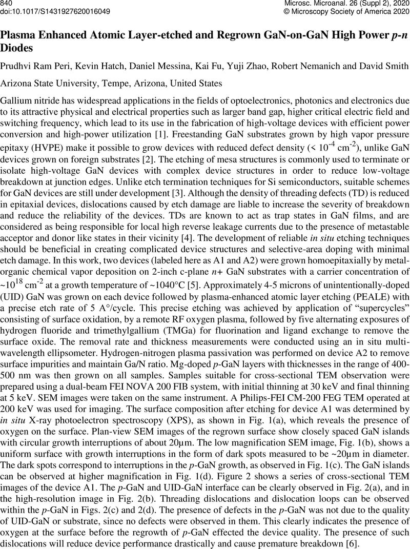
Image of the first page of this content. For PDF version, please use the ‘Save PDF’ preceeding this image.'
Type
Advances in Electron Microscopy to Characterize Materials Embedded in Devices
Copyright
Copyright © Microscopy Society of America 2020

References

Zhao, Y., Fu, H., Wang, G. T., and Nakamura, S., Adv. Opt. Photonics 10, 246 (2018).10.1364/AOP.10.000246CrossRefGoogle Scholar
Kizilyalli, I. C., Edwards, A. P., Aktas, O., Prunty, T., and Bour, D., IEEE Trans. Electron Devices 62, (2015).10.1109/TED.2014.2360861CrossRefGoogle Scholar
Oka, T., Ueno, Y., Ina, T., and Hasegawa, K., (2014).Google Scholar
Hansen, P. J., et al. , Appl. Phys. Lett 72, 2247 (1998).10.1063/1.121268CrossRefGoogle Scholar
Sheu, J. K., Lee, M. L., and Lai, W. C., Appl. Phys. Lett 86, 52103 (2005).10.1063/1.1861113CrossRefGoogle Scholar
This work was supported by ARPA-E award DE-AR0000868. The authors acknowledge the use of facilities within the John M. Cowley Center for High Resolution Electron Microscopy at Arizona State University.Google Scholar