The editors of Microscopy Today congratulate the winners of the sixth Microscopy Today Innovation Awards competition. The ten innovations described below advance microscopy in several areas: light microscopy, scanning probe microscopy, electron microscopy, and hybrid microscopy-analysis methods. These innovations will make microscopy and microanalysis more powerful, more flexible, more productive, and easier to accomplish.
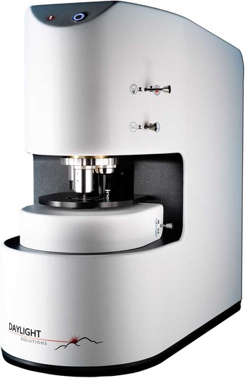
Spero™ Infrared Microscope
Daylight Solutions, Inc.
Developers: Matthew Barre, Miles Weida, Jeremy Rowlette, David Arnone, Benjamin Bird, Edeline Fotheringham, and Timothy Day

Spero™ is a laser-based infrared microscope for collecting analytical data by means of spectral imaging, allowing the user to visualize and identify varying chemical content across a sample with higher spatial resolution, larger fields of view, and shorter acquisition times than existing instruments. Spero is based on Daylight Solutions’s core technology of quantum cascade lasers (QCL). These are compact, semiconductor lasers that are broadly tunable across the “fingerprint region” of the mid-infrared portion of the electromagnetic spectrum, from 5.5 to 11.0 micrometers (1800 cm-1 to 900 cm-1). Infrared light at a single wavelength is transmitted through the sample, and various regions of the sample absorb different portions of the light, providing a 2D spatial map of the sample absorption at that wavelength. The laser is then tuned to an adjacent wavelength, and another image is collected. The resulting hyperspectral data cube stores an entire IR spectrum at each pixel, and this spectrum can be compared against existing spectral libraries to identify the chemical content of each feature in the image.
Chemical imaging can be done in real-time by means of Spero’s Live Mode with the camera running at video frame rates (30 frames per second). This allows the user to view the spatial distribution of specific absorption features, even of dynamic samples such as fluidic flow, chemical reactions, or living organisms.
The fundamental innovation over previous technologies is the use of a tunable QCL illumination source for an IR microscope. Current IR microscopes are based on Fourier Transform Infrared (FTIR) technology, employing a relatively weak broadband illumination source, known as a globar. The Spero microscope provides rapid, high-resolution chemical imaging in minutes that previously took several hours with existing bench-top instruments. Even trips to a synchrotron facility are no longer required because QCL illumination is orders of magnitude brighter than that of a synchrotron.
The Spero IR microscope is already being used in important applications including mapping of ingredients in pharmaceuticals, detecting contaminants in semiconductor manufacturing processes, analyzing the chemistry of polymer films, and screening to detect the earliest stages of cancer in both tissue biopsies and blood serum.
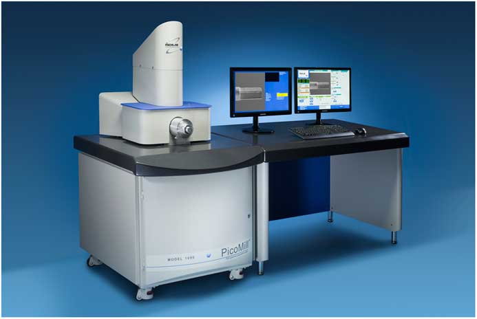
Model 1080 PicoMill® TEM Specimen Preparation System
E.A. Fischione Instruments, Inc.
Developers: Michael Boccabella and Paul Fischione

Advances in aberration-corrected transmission electron microscopy (TEM) demand specimens of higher quality in order to obtain the best high-resolution images. Increased use of focused ion beam (FIB) systems for the preparation of TEM specimens led Fischione Instruments to develop devices to enhance the quality of both conventional and FIB-prepared specimens. The Model 1080 PicoMill® TEM specimen preparation system adds improved imaging capabilities, precise endpoint detection, and better connectivity to the TEM.
The PicoMill provides final thinning of specimens using site-specific, ultra-low-energy, inert gas ion milling. The system’s submicron ionbeam diameter, coupled with a low milling angle, allows targeting of a specific area of interest, prevents redeposition of material onto the specimen surface, and produces uniform thinning of dissimilar materials.
A scanning electron beam provides SEM imaging of the lamella (using either backscattered electrons or secondary electrons) even during ion milling, while the secondary electron detector (SED) also provides ion-beam imaging. An electron detector beneath the specimen enables endpoint detection and quantification of electron transparency. The PicoMill system includes a TEM-style, side-entry goniometer that uses a specially designed specimen holder compatible with most TEMs. This means that a specimen can be transported quickly and safely from the PicoMill system to the TEM without handling.
High-volume enterprises, such as semiconductor manufacturers, frequently employ FIB systems to process a large quantity of TEM specimens. These FIBs use high-energy ions to process specimens quickly, but this often results in specimen damage—amorphization and gallium implantation. For TEM specimens that need the highest quality preparation, the PicoMill system delivers ultra-low ion beam energies (as low as 50 eV) to the specimen.
The PicoMill system is well suited to microelectronics applications. Shrinking sizes and increasingly complex geometries in microelectronic systems, such as three-dimensional FinFET gate architectures and vertical NAND gates, place extra demands on specimen preparation technologies. These devices have dissimilar materials with structures that may contain repeating layers of oxides, silicides, nitrides, and a mix of high-k and low-k dielectric materials. Such devices often employ materials that have very different sputter rates and, at the same time, may possess layer thicknesses of just a few atoms.
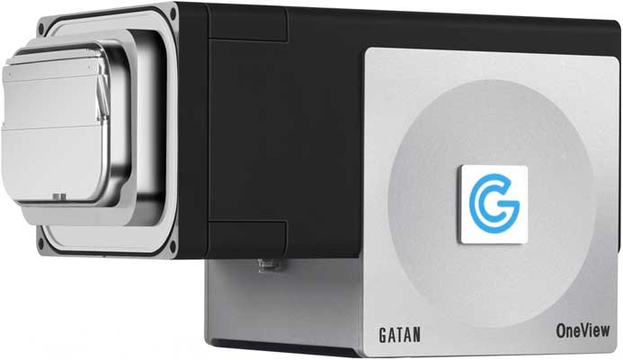
OneView™ Camera
Gatan, Inc.
Developers: Paul Mooney, Matthew Lent, Ed James, and Cory Czarnik

The OneView™ camera captures 4 k × 4 k images at near-TV rates to support a variety of transmission electron microscopy (TEM) applications. Using a proprietary CMOS sensor plus an ultra-fast built-in shutter, individual frame output takes place in 40 ms to permit an acquisition rate of 25 individual frames per second (fps). This ensures a “live” experience when optimizing settings for individual images or acquiring high-speed videos. Users can further define the experimental field of view to allow video recordings over a range of resolution and speed combinations, from 4,096 × 4,096 pixels at 25 fps, to 512 × 512 pixels at 300 fps. Compared to previous technologies, users no longer have to decide between high quality, high frame rate, or high dynamic range. When acquiring a one-second exposure frame, 25 individual frames can be summed together by the OneView camera to create a single image. During acquisition, images can be automatically optimized for exposure time, signal-to-noise ratio, or total specimen dose. The ability to sum frames extends the dynamic range of the final image beyond 16-bits to address the widest range of applications. Combined with a proprietary drift correction algorithm and in-line data processing, individual frames are aligned and then summed in real-time.
Accompanied by a redefined Gatan Microscopy Suite® 3 user interface, the OneView camera features a novel LookBack feature for in-situ applications. When not recording experiments, the camera can be continuously storing live images to disk for up to 20 seconds, allowing pre-record information to be stored to disk when the recording is triggered. This means the user will never miss the start of an experiment again. Up to 15 minutes of continuous video can be stored directly to disk.
The spectrum of applications covers everything from basic bright-field imaging to diffraction (including diffraction movies) and 4D STEM imaging. The camera offers the highest temporal resolution of any scintillator-based camera available today, allowing for a wide range of in-situ applications. OneView is ideal for beam-sensitive materials, including zeolite or cryo-EM samples because the camera can spread a low-dose beam across a large number of frames to minimize specimen damage.
The Nanoworkbench
Klocke Nanotechnik GmbH
Developers: Ivo Burkart, Eva Burkart, David Peters, and Volker Klocke

The Nanoworkbench is most easily described by analogy to light microscopy where at most light microscopes, people work with tools in their hands. Hand-eye coordination allows complex work processes without the user thinking about it. The Nanoworkbench enables hand-eye coordination in vacuum chambers by means of a new technology system that provides positioning at sub-nanometer resolution. The Nanoworkbench employs a comprehensive set of Nanorobotics for sample manipulation, handling, and preparation; while Nano-Sensing provides nano-analytics, topography measurements, precision mechanics, and modular electronics. These functions are combined with automation of the SEM/FIB for easy operation. All individual machine coordinates of the SEM/FIB (field of view, focus point, stage coordinates) and of the Nanorobotics are transformed into a Global Coordinate System. The 1D-Nanofinger® is used as a “scout” to detect sample and tool positions and to store these positions in global coordinates. The SEM/FIB is controlled to move the sample stage, change focus, and alter magnification automatically. Live images from the SEM/FIB are grabbed and transformed into global coordinates. A Live Image Positioning module allows the user to click on a location in the image, and a tool moves there. All modes of the SEM/FIB are controlled together within the Nanoworkbench software.
Most operations executed manually with light optical stereo microscopes can now be done in any SEM/FIB system with a 0.5 nm tool movement resolution over a 20 × 20 mm2 tool stroke. Previously risky vertical movements of tools are now done securely by Nanoworkbench automation. Users can create their own automation by simple teaching algorithms. The Nanoworkbench can be configured with ready-to-use applications software for NanoManipulation, NanoCutting, NanoCleaning, Force-Distance Measurement, NanoProbing, Particle Sorting, Tribology, or TEM Lamella Handling.
Whether a surgeon or a technician working on micromotors, all users have the same tools in their hands: a pair of tweezers, a tip, a scalpel, a needle, a pipette, or an electrode. These few tools cover 90% of possible manipulation tasks accomplished at light microscopes. Nanoworkbench permits complex handling tasks to be done in an SEM/FIB. This is essentially “keyhole surgery” with four tools and an SEM/FIB in synchronous automated operation.
Scanning Ion Microscopy with Low-Energy Lithium Ions
NIST Center for Nanoscale Science and Technology
Developers: Kevin Twedt, Jabez McClelland, Brenton Knuffman, and Adam Steele

This new microscopy method uses a magneto-optical trap ion source (MOTIS) to generate a high-brightness beam of lithium ions. A laser-cooled and trapped cloud of neutral lithium atoms is photoionized and extracted by an electric field to form a highly parallel beam of ions, which is then scanned and focused by conventional scanning microscopy techniques. The source creates brightness in a fundamentally different way from conventional sources: through reducing the transverse temperature of the ion beam to values as low as a few hundred microkelvin. The result is a focused beam of ions with energy between 500 eV and 5 keV and a measured spot size as small as 27 nm.
Image acquisition is accomplished by collecting either secondary electrons (SEs) or backscattered ions as the beam is scanned. Because the primary ions are positively charged, insulating regions of the target charge positively and thus impede the emission of secondary electrons. For SE images the result is very strong contrast between insulating and conducting areas, with insulating regions appearing dark. Backscattered ion images, on the other hand, exhibit markedly different contrast mechanisms in comparison to SE images. In particular they show a significant dependence on target material atomic number. Also low-energy ion beams penetrate the surface far less than high-energy beams, making the technique more surface-sensitive. The technique is generally applicable to over 25 atomic species, including alkalis, alkaline earths, noble gases, and several metals.
Applications of this new type of ion microscopy in secondary electron mode include imaging of difficult, insulating samples, such as carbon nanotube-impregnated epoxy composites and samples where a clear delineation of insulating regions is desired. In backscattered ion detection mode, contrast between phases of various compositions will benefit. The small surface penetration depth allows the study of samples where the topmost few nanometers are of the most interest. Looking beyond imaging, the choice of ionic species enabled by this technology creates opportunities for implantation of specific species with nanoscale resolution. Further applications include implantation of Li+ into battery materials and the extension of traditional focused ion beam capabilities such as milling, circuit editing, beam chemistry, and ion beam lithography.
3D Cell Explorer
Nanolive SA
Developer: Yann Cotte, Sebastien Equis, Christian Depeursinge, Andreas Kern, and Fatih Toy

The 3D Cell Explorer combines holography and rotational scanning to allow measurements of the refractive index distribution within the cell (3D) and over time (4D).
This holographic tomography technique offers a means to probe living cells in their native environment without labels, stains, or interference. Rotational scanning (with 520 nm laser light) allows low-noise 3D reconstructions at a resolution below the diffraction limit of light. The 3D Cell Explorer has a resolution of Δxy = 200 nm and Δz = 500 nm; it generates a 3D image (tomography) in less than a second.
Traditional fluorescence microscopy techniques rely on complicated procedures requiring time-consuming invasive specimen preparation (1–72 hours), which sometimes can be damaging to the cells. The resulting two-dimensional images either have little contrast or are chemically stained with only a few specific colors. With fluorescence techniques researchers need to decide prior to the experiment which cell parts they want to visualize, applying a maximum of two to three stains at the same time. With the 3D Cell Explorer, the refractive index distribution within the cell is measured at each pixel, and the researcher can decide after the experiment which parts of the cell to visualize. The same image data can be analyzed a limitless number of times, and various organelles can be digitally stained in contrasting colors, without interfering with the normal physiology of the cell. The resulting dataset can be rendered in three dimensions in less than a second.
The 3D Cell Explorer offers new imaging possibilities to scientists who have a need to look at their live cells in real-time without specimen preparation or expensive staining procedures. Applications include routine medical procedures such as morphological analysis of sperm cells for in-vitro fertilization or real-time analysis of the reaction of patient cells to a specific drug. For future developments, Nanolive would like to move toward building a portable device for personalized medicine able to automatically evaluate the reaction of a person’s cells to a particular drug or cosmetic product. Other potential uses for the 3D Cell Explorer include research on cell division, cell death, cell-cell interaction, cell differentiation, intra-cellular trafficking, and cellular remodeling processes such as neuronal remodeling before and after synapses.
CryoView MPTM – MultiProbe Low-Temperature SPM
Nanonics Imaging, Ltd.
Developer: Aaron Lewis

The CryoView MP™ is a multiple-probe scanning probe microscopy (SPM) platform designed to study mechanical, spectroscopic, optical, thermal, and electrical properties at low temperatures. By employing up to four individual probes that can be operated independently and simultaneously, the CryoView MP can perform a variety of characterization and transport measurements in situ in combination with light microscopy techniques such as Raman, fluorescence, and near-field scanning optical microscopy (NSOM) in a controlled environment from room temperature down to 10 K. Advanced forms of SPM are enabled for each individual probe, including AFM, KPM, EFM, S-NSOM, NSOM, STM, AFM-Raman, and TERS.
Previously, Raman and photoluminescence measurements would be carried out on one system, with electrical transport done on a separate probe station, and AFM and Kelvin probe measurements performed on a third system. Finding the exact same spot and conditions for each of these measurements is challenging. With CryoView MP the probe and sample are maintained in close contact through tuning-fork-based feedback, a laser-free feedback method providing force sensitivity without optical artifacts. Enclosed in a high-vacuum chamber, the CryoView MP can be pumped down using a rapid cooling mechanism, reaching temperatures down to 10 K.
Applications possible over a range of temperatures include the following: (a) electrical probe station combined with in situ simultaneous Raman characterization, (b) nanoscale transport measurements, where one probe serves as the excitation source and the second probe maps the transport process, (c) chemical lithography with one probe and high-resolution imaging with a second probe, and (d) combined SPM measurements where one probe can perform an advanced SPM measurement while a high-resolution AFM tip maps the same area.
A particular application is the analysis of 2D materials such as graphene, MoS2, BN, NBSe2, metamaterials, and metasurfaces as well as other functional materials such as Si, carbon nanotubes, III-V semiconductors, and quantum dots. In order to fully examine the potential of these materials, multiple characterization methods need to be brought together to provide a complete understanding of their performance. Some of these methods include: nanometric photoconductivity, nanoelectrical characteristics (electronic mobility, charge carriers, etc.), thermal properties, and the quantum Hall effect.
Lens-Free Computational Microscopy for Giga-Pixel 3D Imaging
Aydogan Ozcan of the University of California at Los Angeles
Developers: Aydogan Ozcan, Alon Greenbaum, and Yibo Zhang

Light microscopy examination of microscale features in pathology slides is one of the gold standards for diagnosing disease. The use of conventional light microscopes, however, is often limited because of their relatively high cost; the bulkiness of lens-based optics; and such characteristics as small field of view (FOV), the need for lateral specimen translations, and the need for repeated focus adjustments. The computational lens-free holographic on-chip microscope can mitigate these challenges. This device is based on the solution of the transport of intensity equation to generate an initial phase guess to the multi-height iterative phase retrieval algorithm as well as rotational field transformations implemented in partially coherent in-line holography. This allows the user to perform wide FOV imaging (across 4.5 mm) of pathology samples with image quality sufficient for clinical diagnosis. The holographically reconstructed image can be focused digitally at any depth within the object FOV after image capture. It is also digitally corrected for artifacts arising from uncontrolled tilting and height variations between the sample and sensor planes.
Our results constitute the first demonstration of three-dimensional (3D) pathology slide imaging using on-chip microscopy. Using this lens-free on-chip microscope, the following observations have been made: invasive carcinoma cells were imaged within human breast sections, Papanicolaou smears were analyzed consistent with a high-grade squamous intraepithelial lesion, and sickle cell anemia blood smears were assessed. Blood smears could be examined over a large FOV of 20.5 mm2, more than 100-fold larger than a traditional light microscope. The resulting wide-field lens-free images were shown to have sufficient image resolution and contrast for clinical diagnosis in a blind test by an expert pathologist. Lens-free computational microscopy on a chip could have an important translational impact on the practice of pathology in resource-limited clinical settings. This cost-effective microscope not only records high-quality images over a wide FOV, but also retrieves the complex optical field of the specimen such that the pathologist can digitally adjust the focus of the sample after image capture. This provides a “virtual” depth-of-field experience for investigating sample slides, matching the manual depth adjustment that is routinely practiced in clinical examination of specimens under traditional light microscopes.
Delphi
Phenom-World BV
Developers: Pieter Kruit, Andries Effting, and Sander den Hoedt

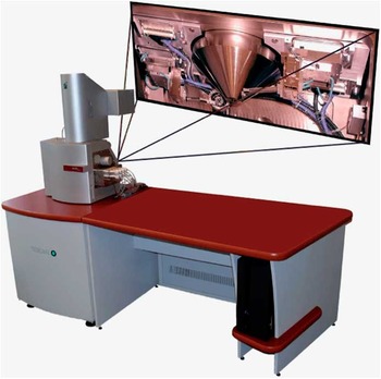
Delphi integrates fluorescence microscopy (FM) and electron microscopy (EM) in a single device by equipping a tabletop scanning electron microscope (SEM) with an inverted fluorescence microscope. This integration enables scientists to correlate two different types of information on the same cell, tissue, or structure of interest. Although correlative light electron microscopy (CLEM) is becoming more popular, the complexity of the workflow has limited its widespread adoption. Delphi makes correlative microscopy more accessible by its compact design and user friendliness.
The inverted fluorescence microscope in the Delphi is placed underneath the electron beam and allows researchers to seamlessly switch between the two imaging modalities. This setup eliminates the need to search for a region of interest (ROI) because the light optical beam and the electron beam are always aligned on the ROI. The integrated design of the Delphi, together with its open-source software package, make the Delphi easy to operate. The intuitive software package allows the user to control all light microscopy settings as well as all SEM settings.
The Delphi comes with a sample holder designed to carry a 14 × 14 mm coverslip. The sample holder has carbon tape corners enabling the user to locate the coverslip in the correct position. The sample is open to the electron beam and transparent to the light beam.
Along with simplifying correlative microscopy, the Delphi reduces correlative workflow time. Sample loading time for the Delphi is about 2 minutes, and, after loading, the user can immediately begin correlative imaging. Precision mechanisms and the use of a proprietary automated alignment technique ensure precise, user-independent overlay of FM and EM images using cathodoluminescence, which is generated as the electron beam hits the glass coverslip.
Application areas are quite broad. The main uses of the Delphi, however, are found in the life sciences where correlative microscopy is getting attention for its ability to combine structural and functional information. For whole cells, Delphi permits the study of cell surface morphology in correlation with specific proteins of interest. Using the Delphi for thin sections allows one to add fluorescent markers that can pinpoint regions of interest, screen large areas, and identify subcellular structures on a molecular basis.
MultiSEM 505
Carl Zeiss Microscopy GmbH
Developers: Dirk Zeidler, Sebastian Vollmar, Arne Thoma, Robert Schwede, Dieter Schumacher, Stefan Schubert, Karin Schiele, Christof Riedesel, Nicole Rauwolf, Stephan Nickell, Mario Mìtzel, Ingo Mìller, Ralf Lenke, Dieter Lechner, Uwe Lang, Jìrgen Kynast, Paul Kortyka, Thomas Kemen, Nicolas Kaufmann, Nico Kämmer, Jörg Jacobi, Tomasz Garbowski, Kevin Flechsler, Anna Lena Eberle, Gregor Dellemann, Christian Crìger, Wilhelm Bolsinger, Michael Behnke, Pascal Anger, and Dirk Aderhold

The MultiSEM 505 multi-beam scanning electron microscope (SEM) images large areas at high resolution by increasing the speed at which SEM data can be acquired by almost two orders of magnitude. It uses multiple electron beams in one electron optical column and employs one detection channel for each beam. The basic principle of operation is the same as with any single-beam SEM, but in the multi-beam SEM the electron source produces an array of 61 electron beams that are focused onto the sample and scanned in parallel 61 small, overlapping subregions of the sample area underneath the beam array. Secondary electrons emanate from each primary electron spot and are imaged onto a multi-detector with one detection channel for each electron beam. An image of an entire large area is produced by the primary beam array in the time it takes one of the 61 beams to scan its small sub-area.
The maximum scan speed is governed by the minimum number of electrons per pixel required to achieve an acceptable signal-to-noise ratio (SNR), which in turn is limited by the speed and efficiency of the secondary electron detector. The electron beam dwell time per pixel is therefore ultimately limited by the bandwidth of the electron detector. Using multiple electron beams in a single column and having a dedicated detector for each beam bypasses the detector bandwidth limit. The multi-beam electron optical design with its comparably low current per individual single beam also minimizes electron beam damage of the sample.
In the past SEMs may not have been considered for applications that require high-throughput imaging. Two important fields requiring such high-throughput at nanometer resolution are microelectronics manufacturing and brain research. For example, as structure sizes in semiconductor devices decrease, there is a need for the detection of particles or pattern defects that are only a few nanometers in diameter. A single-beam SEM can sample only a small fraction of wafer area compared to the MultiSEM. For imaging biological samples with electron microscopy, there is an increasing need to image large volumes of biological tissue at high resolution to gain insight into the functioning of human organs. Examples where MultiSEM could have impact include the understanding of neural circuits and the analysis of extended cellular structures.


