Hostname: page-component-586b7cd67f-g8jcs Total loading time: 0 Render date: 2024-11-26T17:21:39.361Z Has data issue: false hasContentIssue false

The Strategy of Advanced Analysis in Semiconductor Nano-Device: From Nanoprobing to Nanoscopy and Nanoanalysis

Published online by Cambridge University Press:  27 August 2014

LiLung Lai*
Affiliation:
Semiconductor Manufacturing International (Shanghai) Corp.18 Zhangjiang Road, Pudong New Area, Shanghai, PRC

Abstract

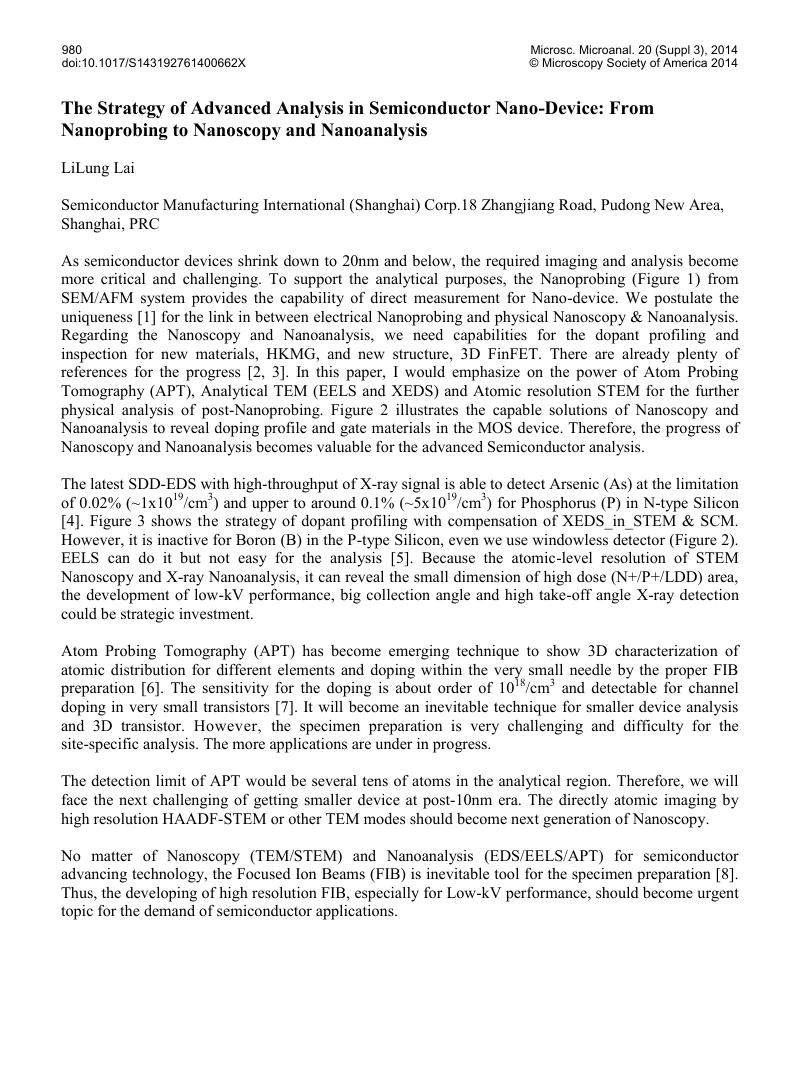
Image of the first page of this content. For PDF version, please use the ‘Save PDF’ preceeding this image.'
Type
Abstract
Copyright
Copyright © Microscopy Society of America 2014 

References

[1] Lai, LL, International Symposium of Testing and Failure Analysis 2013, p.222.Google Scholar
[2] “Transmission Electron Microscopy in Micro-nanoelectronics”, Ed. Alain Claveri, (ISTE) (2012).Google Scholar
[3] Panciera, F et al., Applied Physics Letter 100 (2012), 201909.Google Scholar
[4] Pantel, R, Ultramicroscopy 111 (2011), p.1607.Google Scholar
[5] Duchamp, M et al., Journal of Applied Physics 113 (2013), 093513.Google Scholar
[6] Kambhama, A.K et al., Ultramicroscopy 111 (2011), p.535.Google Scholar
[7] Takamizawa, H. et al., Applied Physics Letter 100 (2012), 25350.Google Scholar