Hostname: page-component-78c5997874-t5tsf Total loading time: 0 Render date: 2024-11-19T12:36:25.419Z Has data issue: false hasContentIssue false

Practical Considerations for Electron Holography on Doped Semiconductor Devices

Published online by Cambridge University Press:  01 August 2002

Alexander Thesen
Affiliation:
EM Facility, University of Tennessee, Knoxville, TN 37996 and High Temperatures Materials Laboratory, Oak Ridge National Laboratory, Bethel Valley Road 1, Oak Ridge, TN 37831
Bernhard G. Frost
Affiliation:
EM Facility, University of Tennessee, Knoxville, TN 37996 and High Temperatures Materials Laboratory, Oak Ridge National Laboratory, Bethel Valley Road 1, Oak Ridge, TN 37831
David C. Joy
Affiliation:
EM Facility, University of Tennessee, Knoxville, TN 37996 and High Temperatures Materials Laboratory, Oak Ridge National Laboratory, Bethel Valley Road 1, Oak Ridge, TN 37831

Abstract

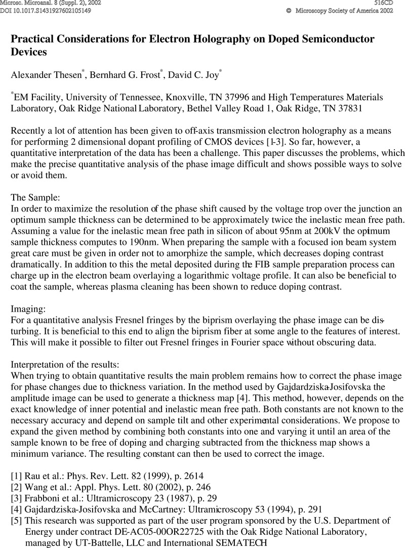
Image of the first page of this content. For PDF version, please use the ‘Save PDF’ preceeding this image.'
Type
Abstract
Copyright
Copyright © Microscopy Society of America 2002