Hostname: page-component-586b7cd67f-g8jcs Total loading time: 0 Render date: 2024-11-26T02:36:25.040Z Has data issue: false hasContentIssue false

Optimization of Image Contrast for Size Distribution Measurements of Nanomaterials by Transmission Electron Microscopies Including TEM and T-SEM

Published online by Cambridge University Press:  27 August 2014

Kazuhiro Kumagai
Affiliation:
Surface and Nano-Analysis Section, Nanomaterial Characterization Division, National Metrology Institute of Japan, National Institute of Advanced Industrial Science and Technology (AIST), TsukubaJapan
Shin-ya Terauchi
Affiliation:
Surface and Nano-Analysis Section, Nanomaterial Characterization Division, National Metrology Institute of Japan, National Institute of Advanced Industrial Science and Technology (AIST), TsukubaJapan
Akira Kurokawa
Affiliation:
Surface and Nano-Analysis Section, Nanomaterial Characterization Division, National Metrology Institute of Japan, National Institute of Advanced Industrial Science and Technology (AIST), TsukubaJapan

Abstract

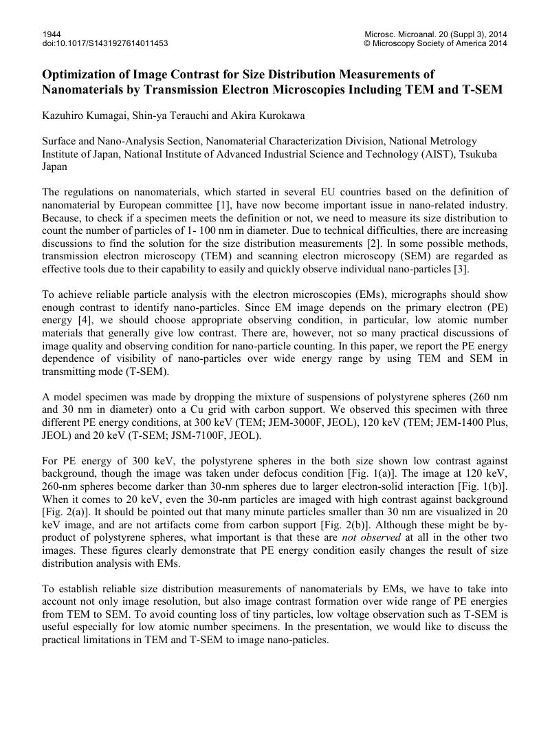
Image of the first page of this content. For PDF version, please use the ‘Save PDF’ preceeding this image.'
Type
Abstract
Copyright
Copyright © Microscopy Society of America 2014 

References

[1] European Commission , Official Journal of the European Union L 275, 20.10.2011 (2011). p. 38.Google Scholar
[2] Lopez-Serrano, A, et al, Analytical Methods 6 (2014) p. 38.Google Scholar
[3] EFSA Scientific Committee, EFSA Journal 9 (2011) 2140.Google Scholar
[4] Reimer, L, Kohl, H Transmission Electron Microscopy: Physics of Image Formation (Springer, (2008).Google Scholar
[5] The authors thank Dr. H. Kato in AIST for kind help in specimen preparation. This work was performed as one of the studies conducted by the consortium for measurement solutions for industrial use of nanomaterials (COMS-NANO) in Japan.Google Scholar