


No CrossRef data available.
Article contents
In situ TEM Approaches to Controlling the Growth of Semiconductors on 2D Materials
Published online by Cambridge University Press: 05 August 2019
Abstract
An abstract is not available for this content so a preview has been provided. As you have access to this content, a full PDF is available via the ‘Save PDF’ action button.
- Type
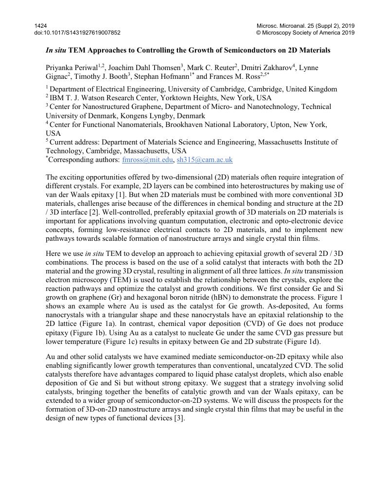
- In situ TEM Characterization of Dynamic Processes During Materials Synthesis and Processing
- Information
- Copyright
- Copyright © Microscopy Society of America 2019
References
[1]Koma., A, Van der Waals epitaxy of lattice-mismatched systems, Journal of Crystal Growth 201 (1999) 236.Google Scholar
[2]Xu., Y, Cheng., C, Du., S, Yang., J, Yu., B, Luo., J, Yin., W, Li., E, Dong., S, Ye., P, Duan., X, Contacts between Two- and Three-Dimensional Materials: Ohmic, Schottky and p-n heterojunctions, ACS Nano 10 (2016) 4895.Google Scholar
[3]We acknowledge financial support from the EPSRC (EP/K016636/1) and ERC (Grant 279342: InSituNANO) (PP, SH) and the Center for Functional Nanomaterials, Brookhaven National Laboratory, which is supported by the U.S. Department of Energy, Office of Basic Energy Sciences, under contract DE-AC02-98CH10886 (DZ). We also acknowledge Dr Mark C. Reuter and Arthur W. Ellis of IBM for their invaluable technical support.Google Scholar
 You have
Access
You have
Access